
Chapter 22: W55MH32’s TIM - Advanced Timer
Chapter 22: W55MH32’s TIM - Advanced Timer
Chapter 22: W55MH32’s TIM - Advanced Timer
Reference materials for this chapter: "W55MH32 Chinese Reference Manual" - Advanced Timer Section. When studying this chapter, it will be more effective to read along with the reference materials, especially for the sections related to register explanations.
1 Advanced Control Timer
The advanced control timers (TIM1 and TIM8) and the general timers have introduced external pins based on the basic timers, enabling input capture and output comparison functions. The advanced control timers have added programmable dead zone complementary output, repetitive counter, and braking (open circuit) functions, which are all for industrial motor control. These functions will not be elaborated in detail in this book; instead, the commonly used input capture and output comparison functions will be mainly introduced.
The advanced control timer timing base unit contains a 16-bit auto-reload register (ARR), a 16-bit counter (CNT), which can count upwards or downwards, a 16-bit programmable prescaler (PSC), and the prescaler clock source has multiple options, including an internal clock and an external clock. There is also an 8-bit repeat counter (RCR), allowing for a maximum of 40-bit programmable timing.
The specific IO allocation for the advanced/general timer of W55MH32 can be found in the table: Advanced Control and General Timer Channel Pin Distribution. The accompanying development board has insufficient IO resources, and many of the IO pins of the timer have been reused for other purposes. Therefore, only a portion of the IOs in the following table can be used for the experiments of the timer.
Advanced Timer | General Timer |
|
|
|
|
|
| TIM1 | TIM8 | TIM2 | TIM5 | TIM3 | TIM4 |
CH1 | PA8/PE9 | PC6 | PA0/PA15 | PA0 | PA6/PC6/PB4 | PB6/PD12 |
CH1N | PB13/PA7/PE8 | PA7 |
|
|
|
|
CH2 | PA9/PE11 | PC7 | PA1/PB3 | PA1 | PA7/PC7/PB5 | PB7/PD13 |
CH2N | PB14/PB0/PE10 | PB0 |
|
|
|
|
CH3 | PA10/PE13 | PC8 | PA2/PB10 | PA2 | PB0/PC8 | PB8/PD14 |
CH3N | PB15/PB1/PE12 | PB1 |
|
|
|
|
CH4 | PA11/PE14 | PC9 | PA3/PB11 | PA3 | PB1/PC9 | PB9/PD15 |
ETR | PA12/PE7 | PA0 | PA0/PA15 |
| PD2 | PE0 |
BKIN | PB12/PA6/PE15 | PA6 |
|
|
|
|
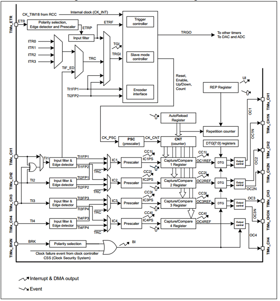
2 Advanced Control Timer Function Block Diagram
The block diagram of the advanced control timer includes the core content of the advanced control timer. By mastering this block diagram, one can have a comprehensive understanding of the advanced control timer. When programming, the thinking will be very clear. Note that some registers in the figure have shadows, indicating that they have shadow registers.
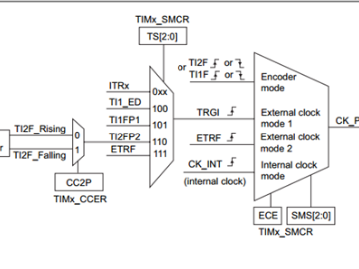
2.1 Clock Selection
The counter clock can be provided by the following clock sources:
Internal clock (CK_INT)
External clock mode 1: External input pin
External clock mode 2: External trigger input ETR
Internal trigger input (ITRx): Use one timer as the prescaler of another timer. For example, a timer Timer1 can be configured as the prescaler of another timer Timer2.
Internal clock source (CK_INT): If the clock source from the mode controller (SMS=000) is disabled, then CEN, DIR (in the TIMx_CR1 register) and UG bit (in the TIMx_EGR register) are de facto control bits, and can only be modified by software (the UG bit is still automatically cleared). As long as the CEN bit is written as '1', the clock of the prescaler is provided by the internal clock CK_INT.
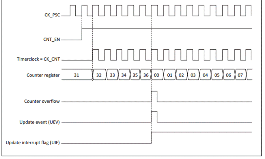
The following figure shows the operation of the control circuit and the up counter in the general mode without a prescaler.
External Clock Source Mode 1
This mode is selected when the SMS bit in the TIMx_SMCR register is set to 111. The counter can count each rising or falling edge of the selected input.
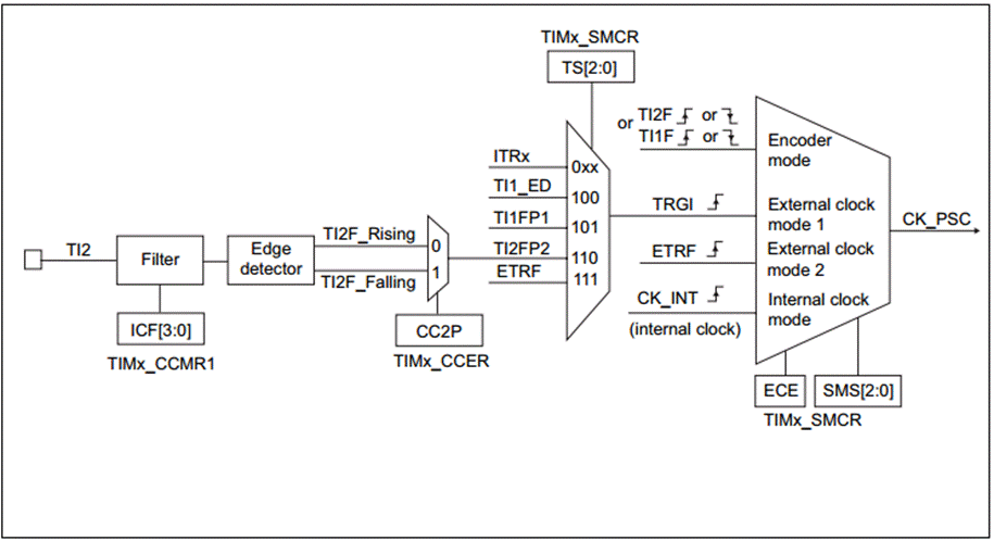
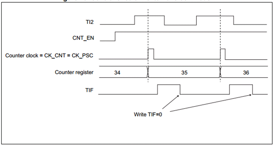
For example, to configure an upward counter to count the rising edge at the input of T12, follow these steps: Configure the TIMx_CCMR1 register with CC2S = 01, configure channel 2 to detect the rising edge of the TI2 input. Configure the IC2F[3:0] of the TIMx_CCMR1 register to select the input filter bandwidth (if no filter is needed, keep IC2F = 0000). Configure the TIMx_CCER register with CC2P = 0, select the rising edge polarity W55MH32 reference manual V1.0.0 201/671. Configure the TIMx_SMCR register with SMS = 111 to select the external clock mode 1 of the timer. Configure the TIMx_SMCR register with TS = 110 to select TI2 as the trigger input source. Set the TIMx_CR1 register with CEN = 1 to start the counter. Note: The capture prescaler does not need to be configured as it is not used as a trigger. Therefore, no configuration is required for it.
When the rising edge occurs at TI2, the counter counts once and the TIF flag is set. The delay between the rising edge of TI2 and the actual clock of the counter depends on the re-synchronization circuit at the TI2 input.
External Clock Source Mode 2
The method to select this mode is: Set the ECE bit in the TIMx_SMCR register to 1. Then the counter can count each rising or falling edge of the ETR signal triggered externally.
The following figure is the block diagram of the external trigger input.
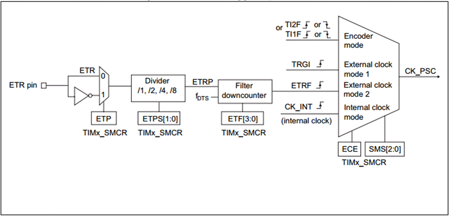
For example, to configure an upward counter that counts once every 2 rising edges under ETR, use the following steps: In this case, no filter is required. Set the ETF[3:0] in the TIMx_SMCR register to 0000 to set the prescaler, set the ETPS[1:0] in the TIMx_SMCR register to 01. Select the rising edge detection of ETR, set ETP in the TIMx_SMCR register to 0 to enable the external clock mode 2, and write TIMx_SMCR.
The ECE in the register is set to 1. Start the counter. Write the CEN=1 value to the TIMx_CR1 register. The counter counts once for every 2 ETR rising edges. The delay between the ETR rising edge and the actual clock of the counter depends on the re-synchronization circuit at the ETRP signal terminal.
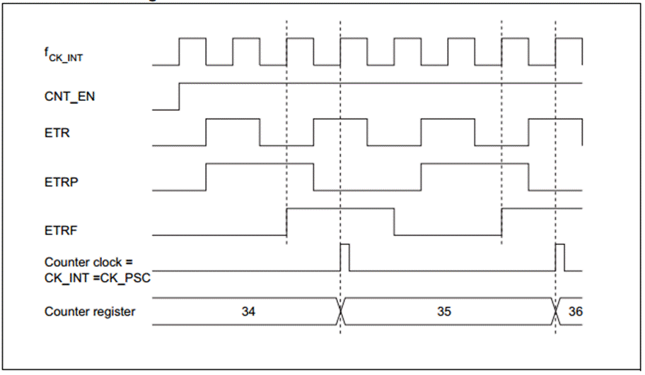
Control circuit in the external clock mode 2
3.5 Capture/Comparison Channel
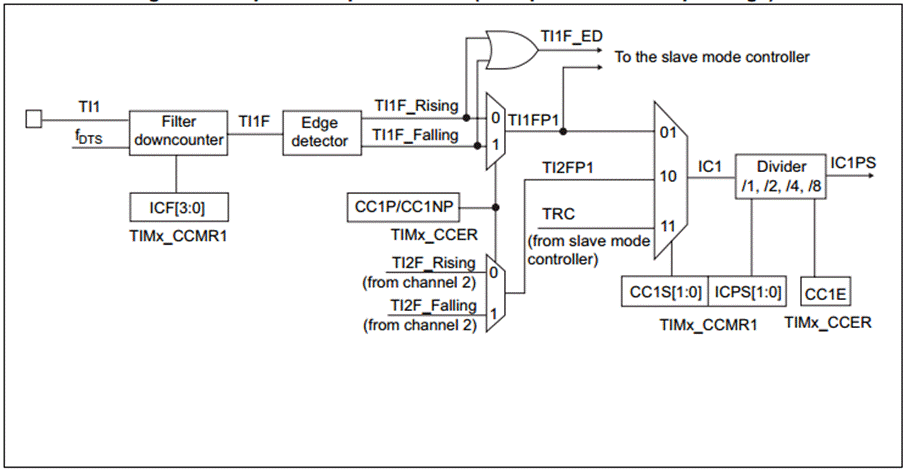
Capture/Comparison Channel (e.g. Channel 1 Input Section)
The output section generates an intermediate waveform OCxRef (high active) as the reference, and the end of the chain determines the polarity of the final output signal.
Capture/Compare Channel 1 Main Circuit
The output section of the capture/comparison channels (channels 1 to 3)
The output section of the capture/comparison channel (Channel 4)
The capture/comparison module consists of a preloading register and a shadow register. The read and write processes only operate on the preloading register. In the capture mode, the capture occurs on the shadow register and is then copied to the preloading register.
In the comparison mode, the contents of the pre-loaded register are copied to the shadow register, and then the contents of the shadow register are compared with the counter.
3.6 Input Capture Mode
In the input capture mode, when the corresponding edge on the ICx signal is detected, the current value of the counter is latched into the capture/comparison register (TIMx_CCRx). When a capture event occurs, the corresponding CCxIF flag (TIMx_SR register) is set to 1. If interrupts or DMA operations are enabled, an interrupt or DMA request will be generated. If the CCxIF flag is already high when a capture event occurs, the repeat capture flag CCxOF (TIMx_SR register) is set to 1. Writing CCxIF = 0 can clear CCxIF, or reading the captured data stored in the TIMx_CCRx register can also clear CCxIF. Writing CCxOF = 0 can clear CCxOF.
The following examples illustrate how to capture the value of the counter when the rising edge of TI1 is detected and store it in the TIMx_CCR1 register. The steps are as follows:
Select the effective input terminal: TIMx_CCR1 must be connected to the TI1 input. Therefore, when writing to the TIMx_CCR1 register, set CC1S = 01. As long as CC1S is not '00', the channel is configured as an input, and the TIMx_CCR1 register becomes read-only.
According to the characteristics of the input signal, configure the input filter to the required bandwidth (that is, when the input is TIx, the input filter control bit is the ICxF bit in the TIMx_CCMRx register). Assuming that the input signal fluctuates within a maximum of 5 internal clock cycles, we must configure the filter's bandwidth to be longer than 5 clock cycles; therefore, we can (at the fDTS frequency) sample 8 times consecutively to confirm a true edge transition on TI1, that is, write IC1F = 0011 in the TIMx_CCMR1 register.
Select the effective conversion edge of the TI1 channel and write CC1P=0 (rising edge) in the TIMx_CCER register.
Configure the input prescaler. In this example, we want to capture the event at every valid level transition, so the prescaler is disabled (write IC1PS=00 in the TIMx_CCMR1 register).
Set CC1E=1 in the TIMx_CCER register to allow the capture counter value to be stored in the capture register.
If necessary, enable the corresponding interrupt request by setting the CC1IE bit in the TIMx_DIER register, and enable the DMA request by setting the CC1DE bit in the TIMx_DIER register.
When an input capture occurs:
When an effective level conversion occurs, the value of the counter is transferred to the TIMx_CCR1 register.
The CC1IF flag is set (interrupt flag). When at least 2 consecutive captures occur and the CC1IF flag has not been cleared, CC1OF is also set to 1.
If the CC1IE bit is set, an interrupt will be generated.
If the CC1DE bit is set, a DMA request will also be generated.
To handle capture overflows, it is recommended to read the capture overflow flag before reading the data. This is to avoid losing the capture overflow information that may be generated after reading the capture overflow flag and before reading the data.
3.7 PWM Input Mode
This mode is a special case of the input capture mode. Apart from the following differences, the operation is the same as that of the input capture mode:
Two ICx signals are mapped to the same TIx input.
These two ICx signals are edge-triggered, but with opposite polarities.
One TIxFP signal is used as the trigger input signal, and the mode controller is configured as the reset mode.
For example, you need to measure the length (in the TIMx_CCR1 register) and duty cycle (in the TIMx_CCR2 register) of the PWM signal input to TI1. The specific steps are as follows (depending on the frequency of CK_INT and the value of the prescaler):
Select the valid input for TIMx_CCR1: Set the CC1S bit in the TIMx_CCMR1 register to 01 (selecting TI1).
Select the valid polarity for TI1FP1 (used to capture data into TIMx_CCR1 and clear the counter): Set CC1P to 0 (rising edge is effective).
Select the valid input for TIMx_CCR2: Set the CC2S bit in the TIMx_CCMR1 register to 10 (selecting TI1).
Select the valid polarity for TI1FP2 (to capture data into TIMx_CCR2): Set CC2P to 1 (falling edge is effective).
Select the valid trigger input signal: Set the TS bit in the TIMx_SMCR register to 101 (selecting TI1FP1).
Configure the mode controller to the reset mode: Set the SMS bit in the TIMx_SMCR to 100.
Enable capture: Set CC1E and CC2E bits in the TIMx_CCER register to 1.
PWM Input Mode Timing
Since only TI1FP1 and TI2FP2 are connected to the slave mode controller, the PWM input mode can only use the TIMx_CH1/TIMx_CH2 signals.
3.8 Output Comparison Mode
This function is used to control an output waveform or to indicate that a given period of time has elapsed. When the counter matches the content of the capture/comparison register, the output comparison function performs the following operations:
The values defined by the output comparison mode (the OCxM bit in the TIMx_CCMRx register) and the output polarity (the CCxP bit in the TIMx_CCER register) are output to the corresponding pins. When a match occurs, the output pin can maintain its level (OCxM = 000), be set to an active level (OCxM = 001), be set to an inactive level (OCxM = 010), or be inverted (OCxM = 011).
The flag in the interrupt status register (the CCxIF bit in the TIMx_SR register) is set.
If the corresponding interrupt mask (the CCxIE bit in the TIMx_DIER register) is set, an interrupt is generated.
If the corresponding enable bit (the CCDE bit in the TIMx_DIER register or the CCDS bit in the TIMx_CR2 register) is set, a DMA request is generated.
The OCxPE bit in TIMx_CCMRx selects whether the TIMx_CCRx register needs to use the preloading register. In the output comparison mode, the update event UEV has no effect on OCxREF and OCx output.
The synchronization accuracy can reach one counting cycle of the counter. The output comparison mode (in the single pulse mode) can also be used to output a single pulse.
Configuration steps for the output comparison mode:
1. Select the counter clock (internal, external, prescaler).
2. Write the corresponding data into the TIMx_ARR and TIMx_CCRx registers.
3. If an interrupt request is to be generated, set the CCxIE bit.
4. Select the output mode, for example:
Require the counter to match CCRx to toggle the output pin of OCx, set OCxM=011
Set OCxPE=0 to disable the preloaded register
Set CCxP=0 to select the polarity as high level effective
Set CCxE=1 to enable the output
5. Set the CEN bit in the TIMx_CR1 register to start the counter
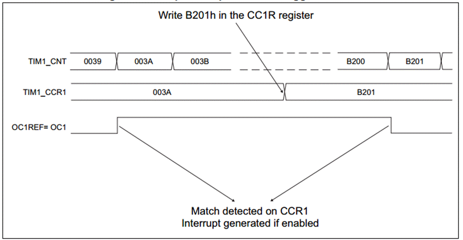
The TIMx_CCRx register can be updated at any time through software to control the output waveform, provided that the preloaded register is not used (OCxPE='0'), otherwise the shadow register of TIMx_CCRx can only be updated when the next update event occurs. The following figure provides an example.
3.9 PWM Mode
The pulse width modulation mode can generate a signal whose frequency is determined by the TIMx_ARR register and whose duty cycle is determined by the TIMx_CCRx register.
By writing '110' (PWM mode 1) or '111' (PWM mode 2) to the OCxM bit in the TIMx_CCMRx register, each OCx output channel can independently generate one PWM signal. The corresponding preload register must be enabled by setting the OCxPE bit in the TIMx_CCMRx register. Finally, the ARPE bit in the TIMx_CR1 register (in up-counting or center-symmetric mode) needs to be set to enable the automatically reloaded preload register.
Only when an update event occurs, can the pre-loaded registers be transferred to the shadow registers. Therefore, before the counter starts counting, all the registers must be initialized by setting the UG bit in the TIMx_EGR register. The polarity of OCx can be set through software in the TIMx_CCER register by setting the CCxP bit. It can be set to be high-level effective or low-level effective. The output enable of OCx is controlled by the combination of the CCxE, CCxNE, MOE, OSSI and OSSR bits (in the TIMx_CCER and TIMx_BDTR registers). In PWM mode (mode 1 or mode 2), TIMx_CNT and TIMx_CCRx are always compared (depending on the counting direction of the counter) to determine whether TIMx_CCRx ≤ TIMx_CNT or TIMx_CNT ≤ TIMx_CCRx.
Based on the status of the CMS bit in the TIMx_CR1 register, the timer can generate a PWM signal that is edge-aligned or a PWM signal that is center-aligned.
PWM edge alignment mode
- Upward Counting Configuration
When the DIR bit in the TIMx_CR1 register is at a low level, the upward counting is executed. Here is an example of PWM mode 1. When TIMx_CNT < TIMx_CCRx, the PWM reference signal OCxREF is high, otherwise it is low. If the comparison value in TIMx_CCRx is greater than the auto-reload value (TIMx_ARR), then OCxREF remains at '1'. If the comparison value is 0, then OCxREF remains at '0'. The following is an example of a PWM waveform with edge alignment when TIMx_ARR = 8.
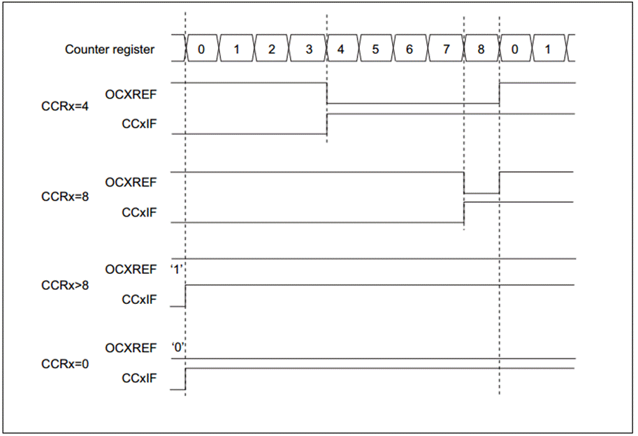
Edge-aligned PWM waveform (ARR = 8)
- Configuration for decrementing in a downward direction
When the DIR bit in the TIMx_CR1 register is at a high level, the decrementing operation is performed. In PWM mode 1, when TIMx_CNT > TIMx_CCRx, the reference signal OCxREF is low; otherwise, it is high. If the comparison value in TIMx_CCRx is greater than the auto-reload value in TIMx_ARR, then OCxREF remains at '1'. In this mode, a 0% PWM waveform cannot be generated.
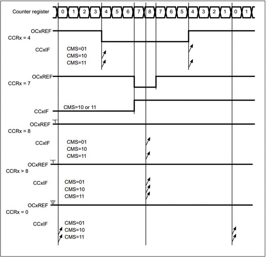
PWM Center Alignment Mode
When the CMS bit in the TIMx_CR1 register is not '00', it is in the center-aligned mode (all other configurations have the same effect on the OCxREF/OCx signals). Depending on the different CMS bit settings, the compare flag can be set to 1 when the counter is counting upwards, when it is counting downwards, or when it is counting both upwards and downwards. The count direction bit (DIR) in the TIMx_CR1 register is updated by hardware and should not be modified by software. The following figure provides some examples of central-aligned PWM waveforms.
TIMx_ARR=8
PWM Mode 1
In the TIMx_CR1 register, when CMS is set to 01 and in the central alignment mode 1, the compare flag is set when the counter is decrementing.
Hint for using the center alignment mode:
When entering the center alignment mode, use the current upward/downward counting configuration; this means that whether the counter counts upward or downward depends on the current value of the DIR bit in the TIMx_CR1 register. Additionally, the software cannot simultaneously modify the DIR and CMS bits.
It is not recommended to rewrite the counter while running in the center alignment mode because this can lead to unpredictable results. Specifically: If the value written to the counter is greater than the auto-reload value (TIMx_CNT > TIMx_ARR), the direction will not be updated. For example, if the counter is counting upward, it will continue to do so. If 0 or the value of TIMx_ARR is written to the counter, the direction is updated, but no update event UEV is generated.
The safest way to use the center alignment mode is to generate a software update (set the UG bit in the TIMx_EGR register) before starting the counter, and do not modify the counter's value during the counting process.
3.10 Complementary Output and Dead Zone Insertion
The advanced control timers (TIM1 and TIM8) can output two complementary signals and manage the instantaneous switching on and off of the outputs. This period is commonly referred to as the dead zone. Users should adjust the dead zone time according to the connected output devices and their characteristics (such as the delay of level conversion, the delay of power switch, etc.).
By configuring the CCxP and CCxNP bits in the TIMx_CCER register, the polarity (either the main output OCx or the complementary output OCxN) can be independently selected for each output.
The complementary signals OCx and OCxN are controlled by the combination of the following control bits: the CCxE and CCxNE bits in the TIMx_CCER register, the MOE, OISx, OISxN, OSSI and OSSR bits in the TIMx_BDTR and TIMx_CR2 registers. In particular, the dead time is activated when transitioning to the IDLE state (MOE drops to 0).
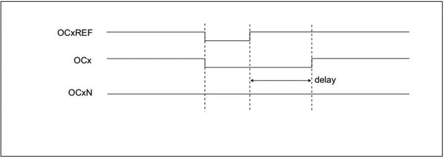
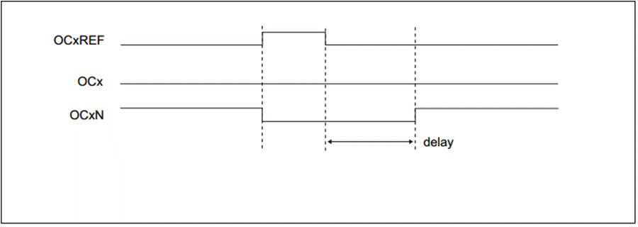
Simultaneously setting the CCxE and CCxNE bits will insert a dead zone. If there is a brake circuit, the MOE bit also needs to be set. Each channel has a 10-bit dead zone generator. The reference signal OCxREF can generate two outputs OCx and OCxN. If OCx and OCxN are high-active:
The output signal of OCx is the same as the reference signal, except that its rising edge has a delay relative to the rising edge of the reference signal.
The output signal of OCxN is opposite to the reference signal, except that its rising edge has a delay relative to the falling edge of the reference signal. If the delay is greater than the current effective output width (OCx or OCxN), no corresponding pulse will be generated. The following several figures show the relationship between the output signal of the dead-time generator and the current reference signal OCxREF. (Assume CCxP = 0, CCxNP = 0, MOE = 1, CCxE = 1, and CCxNE = 1)
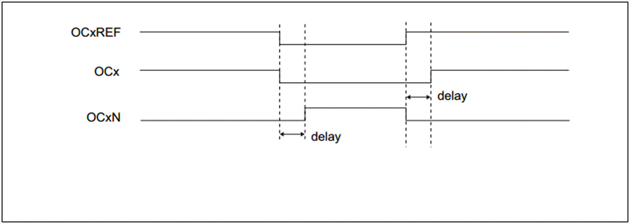
Complementary output with dead zone insertion
Dead zone waveform delay is greater than the negative pulse.
Dead zone waveform delay is greater than the positive pulse.
The dead-time delay for each channel is the same and is programmed by the DTG bit in the TIMx_BDTR register. Redirecting OCxREF to OCx or OCxN
In the output mode (forced output, output comparison or PWM), by configuring the CCxE and CCxNE bits in the TIMx_CCER register, OCxREF can be redirected to the output of OCx or OCxN.
This function can send a special waveform (such as PWM or a static valid level) on a particular output when the complementary output is in an invalid state. Another function is to make both outputs be in an invalid state, or be in an invalid state and a complementary output with dead time.
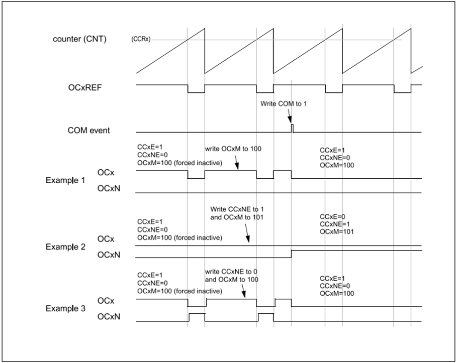
3.11 Generate six-step PWM output
When complementary outputs are required on a channel, the pre-load bits include OCxM, CCxE and CCxNE. When a COM phase change event occurs, these pre-load bits are transferred to the shadow register bits. Thus, you can preset the next step configuration in advance and simultaneously modify the configurations of all channels at the same time. COM can be generated by software by setting the COM bit in the TIMx_EGR register, or by hardware on the TRGI rising edge.
When a COM event occurs, a flag bit (the COMIF bit in the TIMx_SR register) will be set. At this time, if the COMIE bit in the TIMx_DIER register has been set, an interrupt will be generated; if the COMDE bit in the TIMx_DIER register has been set, a DMA request will be generated.
The figure below shows the OCx and OCxN outputs under three different configurations when a COM event occurs.
3.12 Single Pulse Mode
The single pulse mode (OPM) is a special case of the numerous modes mentioned above. This mode allows the counter to respond to an excitation and generate a pulse with a programmable pulse width after a programmable delay. Waveforms can be generated by starting the counter from the mode controller in either the output comparison mode or the PWM mode. Setting the OPM bit in the TIMx_CR1 register will select the single pulse mode, allowing the counter to automatically stop when the next update event UEV is generated.
A pulse is generated only when the comparison value is different from the initial value of the counter. Before starting (when the timer is waiting for a trigger),
the following configuration is required:
Up-counting mode: Counter CNT<CCRx≤ARR (particularly, 0<CCRx),
Down-counting mode: Counter CNT>CCRx.
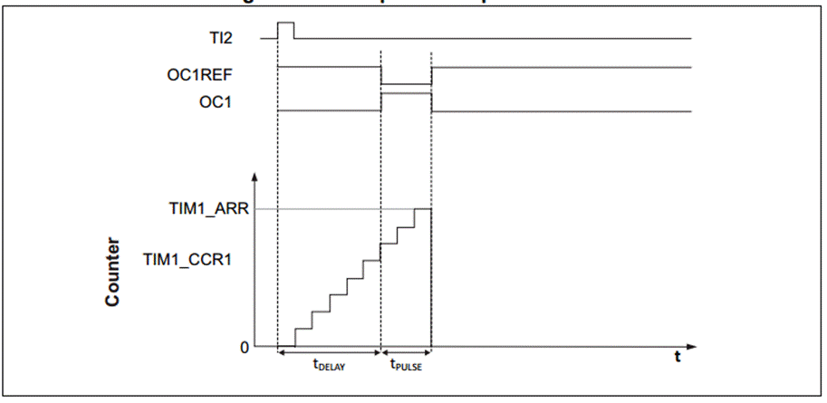
For example, you need to generate a positive pulse of length tPULSE on OC1 after a delay of tDELAY following the detection of an rising edge on the input pin of TI2.
Assume that TI2FP2 serves as trigger 1:
Set the CC2S bit in the TIMx_CCMR1 register to 01, map TI2FP2 to TI2.
Set the CC2P bit in the TIMx_CCER register to 0, so that TI2FP2 can detect the rising edge.
Set the TS bit in the TIMx_SMCR register to 110, making TI2FP2 the trigger (TRGI) of the slave mode controller.
Set the SMS bit in the TIMx_SMCR register to 110 (trigger mode), using TI2FP2 to start the counter. The waveform of OPM is determined by the value written to the comparison register (consider the clock frequency and the counter prescaler).
tDELAY is defined by the value in the TIMx_CCR1 register.
tPULSE is defined by the difference between the auto-load value and the comparison value (TIMx_ARR - TIMx_CCR1).
Assume that a waveform from 0 to 1 is to be generated when a comparison match occurs, and a waveform from 1 to 0 is to be generated when the counter reaches the auto-load value; first set the OC1M bit in the TIMx_CCMR1 register to 111 to enter PWM mode 2; selectively enable the auto-load register as needed: set the OC1PE bit in the TIMx_CCMR1 register to 1 and the ARPE bit in the TIMx_CR1 register; then fill the comparison value in the TIMx_CCR1 register, the auto-load value in the TIMx_ARR register, and set the UG bit to generate an update event, and then wait for an external trigger event on TI2. In this example, CC1P = 0.
In this example, the DIR and CMS bits in the TIMx_CR1 register should be set low. Since only one pulse is required, the TIMx_CR1 register must be set with OPM = 1 to stop counting when the counter flips from the auto-load value to 0 in the next update event.
Special case: OCx rapid enable:
In single pulse mode, the logic at the TIx input pin detects the CEN bit to start the counter. Then the comparison operation between the counter and the comparison value generates the output transition. However, these operations require a certain number of clock cycles, thus limiting the minimum delay tDELAY that can be achieved. If you want to output the waveform with the minimum delay, you can set the OCxFE bit in the TIMx_CCMRx register; in this case, OCxREF (and OCx) directly respond to the excitation without relying on the comparison result, and the output waveform is the same as the waveform when the comparison matches. OCxFE only works when the channels are configured in PWM1 and PWM2 modes.
3.13 Encoder Interface Mode
The method for selecting the encoder interface mode is as follows: If the counter only counts on the rising edge of TI2, then set the SMS bit in the TIMx_SMCR register to 001; if it only counts on the rising edge of TI1, then set SMS to 010; if the counter counts on both the rising edge of TI1 and TI2, then set SMS to 011.
By setting the CC1P and CC2P bits in the TIMx_CCER register, the polarities of TI1 and TI2 can be selected; if necessary, the input filter can also be programmed.
The two inputs TI1 and TI2 are used as interfaces for the incremental encoder. Refer to Table 71. Assuming that the counter has been started (CEN = 1 in the TIMx_CR1 register), the counter is driven by each valid transition on TI1FP1 or TI2FP2. TI1FP1 and TI2FP2 are the signals of TI1 and TI2 after passing through the input filter and polarity control; if there is no filtering and inversion, then TI1FP1 = TI1 and TI2FP2 = TI2. Based on the transition sequence of the two input signals, counting pulses and direction signals are generated. According to the transition sequence of the two input signals, the counter counts up or down, and the hardware sets the corresponding DIR bit in the TIMx_CR1 register. Regardless of whether the counter counts based on TI1, TI2, or both TI1 and TI2, the transition at either input terminal (TI1 or TI2) will re-calculate the DIR bit.
The encoder interface mode is basically equivalent to using an external clock with direction selection. This means that the counter only counts continuously between 0 and the auto-load value of the TIMx_ARR register (depending on the direction, either from 0 to the ARR value, or from ARR to 0). Therefore, TIMx_ARR must be configured before starting the count. Similarly, the capture, comparator, prescaler, repeat counter, trigger output characteristics, etc. still work as normal. The encoder mode and the external clock mode 2 are incompatible, so they cannot be operated simultaneously. In this mode, the counter is automatically modified according to the speed and direction of the incremental encoder, so the content of the counter always indicates the position of the encoder. The counting direction corresponds to the rotation direction of the connected sensor. The following table lists all possible combinations, assuming that TI1 and TI2 do not change simultaneously.
Effective edge | The level of the relative signal (TI1FP1 corresponds to TI2, and TI2FP2 corresponds to TI1) | TI1FP1 signal | TI2FP2 signal |
|
|
|
| Rise | Descend | Rise | Descend |
Only in TI1 count | High | Counting down | Counting upwards | Counting not applicable | Counting not applicable |
| Low | Counting upwards | Counting down | Counting not applicable | Counting not applicable |
Only in TI2 count | High | Counting not applicable | Counting not applicable | Counting upwards | Counting down |
| Low | Counting not applicable | Counting not applicable | Counting down | Counting upwards |
Count on TI1 and TI2 | High | Counting down | Counting upwards | Counting upwards | Counting down |
| Low | Counting upwards | Counting down | Counting down | Counting upwards |
An external incremental encoder can be directly connected to the MCU without the need for external interface logic. However, a comparator is usually used to convert the differential output of the encoder into a digital signal, which significantly enhances the anti-noise interference capability. The third signal output by the encoder indicates the mechanical zero point, and it can be connected to an external interrupt input and trigger a counter reset.
The figure below is an example of a counter operation, showing the generation of the counting signal and the direction control. It also shows how the input jitter is suppressed when the two-edge mode is selected; the jitter can occur when the sensor is positioned close to a transition point. In this example, we assume the configuration as follows:
CC1S='01' (TIMx_CCMR1 register, IC1FP1 mapped to TI1)
CC2S='01' (TIMx_CCMR2 register, IC2FP2 mapped to TI2)
CC1P='0' (TIMx_CCER register, IC1FP1 not inverted, IC1FP1 = TI1)
CC2P='0' (TIMx_CCER register, IC2FP2 not inverted, IC2FP2 = TI2)
SMS='011' (TIMx_SMCR register, all inputs are valid on rising and falling edges)
CEN='1' (TIMx_CR1 register, counter enabled)
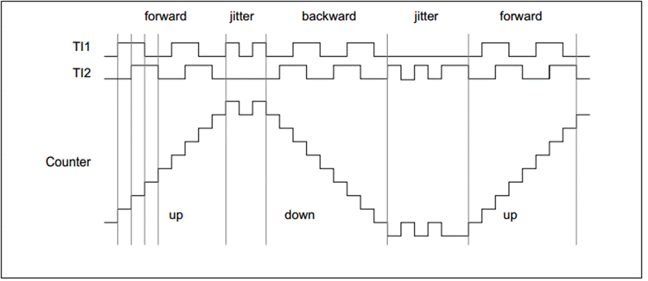
Example of counter operation in encoder mode
The figure below shows the operation example of the counter when IC1FP1 is in inverted polarity (CC1P = '1', other configurations are the same as the previous example)
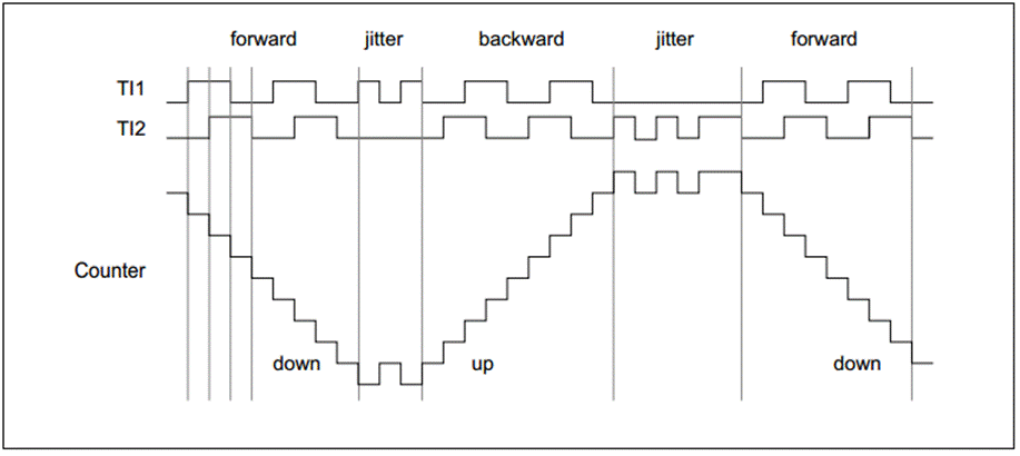
IC1FP1 Inverted Encoder Interface Mode Example
When the timer is configured in the encoder interface mode, it provides information about the current position of the sensor. By using the second timer in the capture mode, the interval between two encoder events can be measured, allowing for the acquisition of dynamic information (velocity, acceleration, deceleration). The encoder output indicating the mechanical zero point can be used for this purpose. Based on the interval between the two events, the counter can be read at fixed intervals. If possible, you can latch the counter value into the third input capture register (the capture signal must be periodic and can be generated by another timer); or you can read its value through a DMA request generated by the real-time clock.
3.14 Timer Input XOR Function
The TI1S bit in the TIMx_CR2 register enables the input filter of channel 1 to be connected to the output terminal of an XOR gate. The three input terminals of the XOR gate are TIMx_CH1, TIMx_CH2, and TIMx_CH3.
The XOR output can be used for all the input functions of the timers, such as triggering or input capture. The next section 23.3.18 provides an example of this feature being used to connect Hall sensors.
3.15 Interface with Hall Sensor
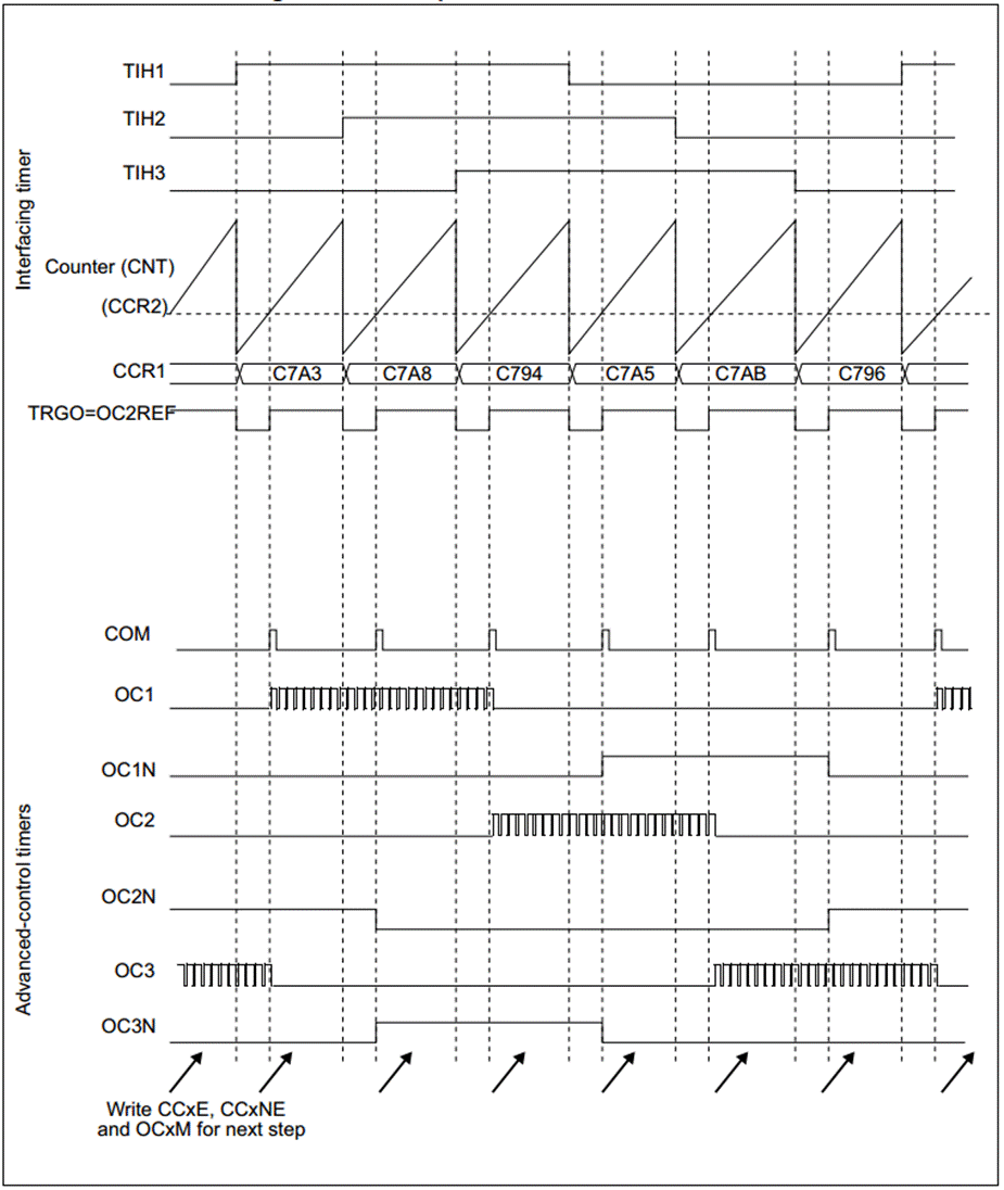
When using the advanced control timer (TIM1 or TIM8) to generate PWM signals to drive the motor, another general TIMx (TIM2, TIM3, TIM4, or TIM5) timer can be used as an "interface timer" to connect the Hall sensor. The three input pins (CC1, CC2, CC3) of the "interface timer" are connected to the TI1 input channel through an XOR gate (by setting the TI1S bit in the TIMx_CR2 register to select), and the "interface timer" captures this signal.
From the mode controller being configured in the reset mode, the input is TI1F_ED. Whenever one of the three inputs changes, the counter restarts from 0 and starts counting anew. This generates a time reference triggered by any change in the Hall input.
The capture/comparison channel 1 on the "interface timer" is configured in capture mode, with the captured signal being TRC. The captured value reflects the time delay between the two input changes and provides information about the motor speed.
The "interface timer" can be used to generate a pulse in the output mode, which can (by triggering a COM event) be used to change the properties of various channels of the high-level timer TIM1 or TIM8, while the high-level control timer generates PWM signals to drive the motor. Therefore, the channel of the "interface timer" must be programmed to generate a positive pulse after a specified delay (output comparison or PWM mode), which is sent to the high-level control timer TIM1 or TIM8 through the TRGO output.
Example: The Hall input is connected to the TIMx timer, and the PWM configuration of the high-level control timer TIMx is changed at a specified moment after any change in any of the Hall inputs.
Set the TI1S bit in the TIMx_CR2 register to '1', configure the three timer inputs as logical OR to TI1,
Timing programming: Set TIMx_ARR to its maximum value (the counter must be reset by the change of TI1). Set the prescaler to obtain the largest counter period, which is longer than the time interval between two changes on the sensor.
Set channel 1 to capture mode (select TRC): Set the CC1S in the TIMx_CCMR1 register to 01. If necessary, the digital filter can also be set.
Set channel 2 to PWM2 mode with the required delay: Set the OC2M in the TIMx_CCMR1 register to 111 and CC2S to 00.
Select OC2REF as the trigger output on TRGO: Set the MMS in the TIMx_CR2 register to 101. In the high-level control register TIM1, the correct ITR input must be the trigger input, and the timer is programmed to generate PWM signals, the capture/comparison control signal is preloaded (CCPC in the TIMx_CR2 register is 1), and the trigger input controls the COM event (CCUS in the TIMx_CR2 register is 1). After a COM event, write the next PWM control bit (CCxE, OCxM), which can be achieved in the interrupt subroutine handling the rising edge of OC2REF.
The following figure shows this example
3.16 Synchronization of TIMx Timer and External Trigger
The TIMx timer can synchronize with an external trigger in multiple modes: reset mode, gating mode and trigger mode.
From mode: Reset mode
When a triggering input event occurs, the counter and its prescaler can be reinitialized; simultaneously, if the URS bit in the TIMx_CR1 register is low, an update event UEV is generated; then all the preloaded registers (TIMx_ARR, TIMx_CCRx) are updated.
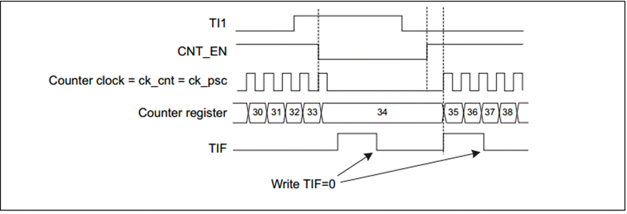
In the following example, the rising edge of the TI1 input port causes the upward counter to be reset:
Configure channel 1 to detect the rising edge of TI1. Configure the bandwidth of the input filter (in this case, no filter is needed, so IC1F = 0000). No capture prescaler is used in the triggering operation, so no configuration is required. The CC1S bit only selects the input capture source, that is, in the TIMx_CCMR1 register, CC1S = 01. Set the TIMx_CCER register to CC1P = 0 to determine the polarity (only detect the rising edge).
Set the TIMx_SMCR register to SMS = 100 to configure the timer in reset mode; Set the TIMx_SMCR register to TS = 101 to select TI1 as the input source.
Set the TIMx_CR1 register to CEN = 1 to start the counter.
The counter begins to count based on the internal clock and then operates normally until a rising edge of TI1 occurs; at this time, the counter is reset and starts counting from 0 again. At the same time, the trigger flag (the TIF bit in the TIMx_SR register) is set. Depending on the settings of the TIE (interrupt enable) and TDE (DMA enable) bits in the TIMx_DIER register, an interrupt request or a DMA request is generated.
The figure below shows the action when the automatic reload register TIMx_ARR is set to 0x36. The delay between the rising edge of TI1 and the actual reset of the counter depends on the re-synchronization circuit at the input end of TI1.
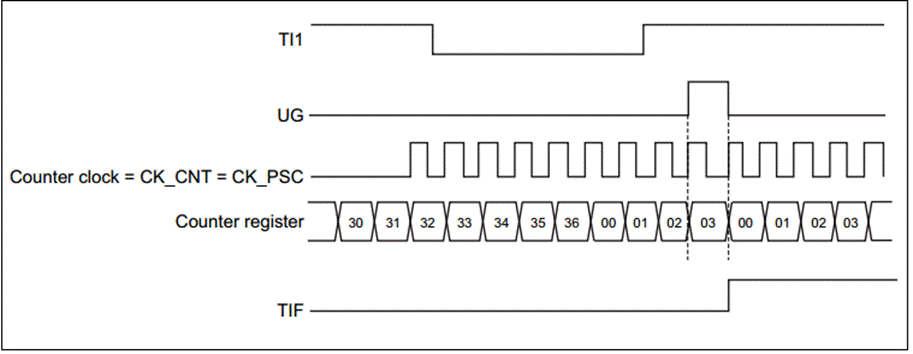
Control circuit in reset mode
From mode: Gate control mode
Enable the counter based on the selected input level. In the following example, the counter increments only when TI1 is low:
Configure channel 1 to detect the low level on TI1. Set the input filter bandwidth (in this case, no filtering is needed, so keep IC1F = 0000). Since no capture prescaler is used in the trigger operation, no configuration is required. The CC1S bit is used to select the input capture source, setting the TIMx_CCMR1 register such that CC1S = 01. Set the TIMx_CCER register such that CC1P = 1 to determine the polarity (only detect the low level).
Set the TIMx_SMCR register such that SMS = 101 to configure the timer in gated mode; set the TIMx_SMCR register such that TS = 101 to select TI1 as the input source.
Set the TIMx_CR1 register such that CEN = 1 to start the counter. In gated mode, if CEN = 0, the counter cannot be started, regardless of the trigger input level.
As long as TI1 is low, the counter starts counting based on the internal clock and stops counting once TI1 goes high. When the counter starts or stops, set the TIF bit in TIMx_SR. The delay between the rising edge of TI1 and the actual stop of the counter depends on the re-synchronization circuit at the TI1 input terminal.
Control circuit in gated mode
From mode: Trigger mode
The selected event enables the counter on the input terminal. In the following example, the counter starts to count upwards from the rising edge of TI2 input:
Configure channel 2 to detect the rising edge of TI2. Configure the input filter bandwidth (in this case, no filter is needed, keep IC2F = 0000). No capture prescaler is used in the trigger operation, no configuration is required. The CC2S bit is only used to select the input capture source, set TIMx_CCMR1 register to CC2S = 01. Set TIMx_CCER register to CC2P = 1 to determine the polarity (only detect low levels).
Set TIMx_SMCR register to SMS = 110 to configure the timer as trigger mode; Set TIMx_SMCR register to TS = 110 to select TI2 as the input source. When a rising edge of TI2 occurs, the counter starts to count under the internal clock drive, and the TIF flag is set. The delay between the TI2 rising edge and the start of counter counting depends on the re-synchronization circuit at the TI2 input terminal.
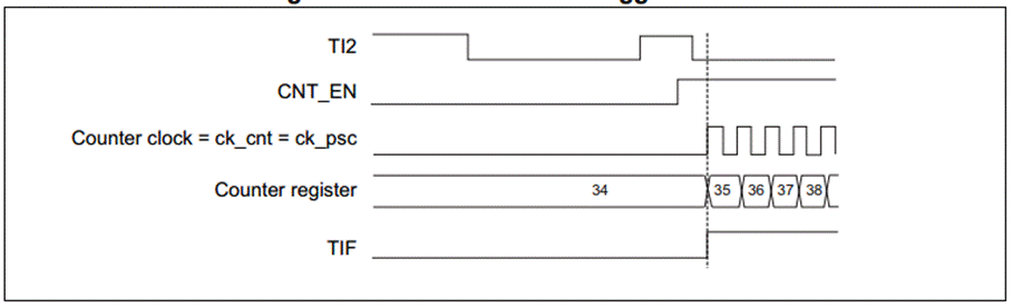
Control circuit in trigger mode
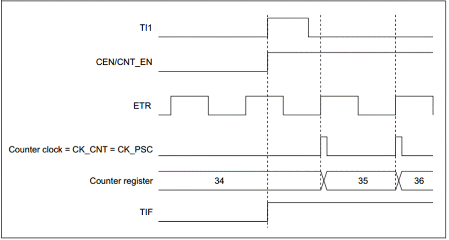
From mode: External clock mode 2 + trigger mode
External clock mode 2 can be used together with another from mode (except for external clock mode 1 and encoder mode). In this case, the ETR signal is used as the input of the external clock, and in reset mode, gated mode or trigger mode, another input can be selected as the trigger input. It is not recommended to use the TS bit of the TIMx_SMCR register to select ETR as TRGI.
In the following example, once an upward edge appears on TI1, the counter counts once for each upward edge of ETR:
1. Configure the external trigger input circuit through the TIMx_SMCR register:
ETF = 0000: No filtering
ETPS = 00: No pre-divider
ETP = 0: Detect the upward edge of ETR, set ECE = 1 to enable external clock mode 2.
2. Configure channel 1 as follows to detect the upward edge of TI:
IC1F = 0000: No filtering
During the trigger operation, the capture pre-divider is not used, and no configuration is required
Set the TIMx_CCMR1 register to CC1S = 01 to select the capture source
Set the TIMx_CCER register to CC1P = 0 to determine the polarity (only detect the upward edge)
3. Set the TIMx_SMCR register to SMS = 110 to configure the timer as trigger mode. Set the TIMx_SMCR register to TS = 101 to select TI1 as the input source. When an upward edge appears on TI1, the TIF flag is set, and the counter starts counting at the upward edge of ETR. The delay between the upward edge of the ETR signal and the actual reset of the counter depends on the re-synchronization circuit at the ETRP input terminal.
4. Detailed Explanation of Timer Initialization Structure
In the standard library function header file w55mh32_tim.h, four initialization structures for the timer peripheral are established, namely the time base initialization structure TIM_TimeBaseInitTypeDef, the output comparison initialization structure TIM_OCInitTypeDef, the input capture initialization structure TIM_ICInitTypeDef, and the break and dead zone initialization structure TIM_BDTRInitTypeDef. Advanced control timers can use all these initialization structures, while general timers cannot use the TIM_BDTRInitTypeDef structure. Basic timers can only use the time base structure. Next, we will explain these four structures in detail.
4.1 TIM_TimeBaseInitTypeDef
The TIM_TimeBaseInitTypeDef structure is used for setting the basic parameters of the timer and is used in conjunction with the TIM_TimeBaseInit function to complete the configuration.
Code Listing: Advanced Timer - 1 Timer Basic Initialization Structure
![]()
TIM_Prescaler: Timer prescaler setting. The clock source through this prescaler becomes the timer's counting clock CK_CNT, and it sets the value of the PSC register. The calculation formula is: the counter clock frequency (fCK_CNT) is equal to fCK_PSC / (PSC[15:0] + 1), which can achieve a 1 to 65536 division ratio.
TIM_CounterMode: Timer counting mode, which can be set to upward counting, downward counting, or center-aligned. The advanced control timer allows the selection of any one of these.
TIM_Period: Timer period, which actually sets the value of the automatic reload register ARR. ARR is the value to be loaded into the actual automatic reload register (i.e., the shadow register), and the setting range is from 0 to 65535.
TIM_ClockDivision: Clock division, setting the division ratio between the timer clock CK_INT frequency and the dead-time generator as well as the sampling clock frequency of the digital filter. You can choose 1, 2, or 4 divisions.
TIM_RepetitionCounter: Repetition counter, only 8 bits, exists only in the advanced timer.
4.2 TIM_OCInitTypeDef
The output comparison structure TIM_OCInitTypeDef is used to specify the comparison mode and is used in conjunction with the TIM_OCxInit function to complete the initialization configuration of the specified timer output channel. The advanced control timer has four timer channels, and each of them must be set independently when used.
Code Listing: Advanced Timer - 2 Timer Compare Output Initialization Structure
1. TIM_OCMode: This selects the output mode, with a total of eight options. The commonly used ones are PWM1/PWM2. It sets the values of the OCxM[2:0] bits in the CCMRx register.
2. TIM_OutputState: This determines the output enable, deciding whether the final output comparison signal OCx is output through an external pin. It sets the values of the CCxE/CCxNE bits in the TIMx_CCER register.
3. TIM_OutputNState: This determines the complementary output enable, deciding whether the complementary signal OCxN is output through an external pin. It sets the value of the CCER register's CCxNE bit.
4. TIM_Pulse: This compares the output pulse width. It actually sets the value of the CCR register to determine the pulse width. The range that can be set is from 0 to 65535.
5. TIM_OCPolarity: This selects the output polarity. It can be set to be high level effective or low level effective. It determines the effective level of the timer channel. It sets the value of the CCxP bit in the CCER register.
6. TIM_OCNPolarity: This compares the complementary output polarity. It can be set to be high level effective or low level effective. It sets the value of the CCxNP bit in the TIMx_CCER register.
7. TIM_OCIdleState: This sets the output level of the channel in the idle state. It can be set to output 1 or 0, that is, after the dead time, the timer channel outputs a high level or low level in the idle state (when BDTR_MOE bit is 0). It sets the value of the OISx bit in the CR2 register.
8. TIM_OCNIdleState: This sets the complementary channel output level in the idle state. It can be set to output 1 or 0, that is, after the dead time, the timer complementary channel outputs a high level or low level. The setting value must be opposite to that of TIM_OCIdleState. It sets the value of the OISxN bit in the CR2 register.
4.2 TIM_ICInitTypeDef
The input capture structure body TIM_ICInitTypeDef is used for the input capture mode and is used in conjunction with the TIM_ICInit function to complete the initialization configuration of the timer input channel. If the PWM input mode is used, it needs to be used in conjunction with the TIM_PWMIConfig function to complete the initialization configuration of the timer input channel.
Code Listing: Advanced Timer Timer Input Capture Initialization Structure
TIM_Channel: Capture channel selection, among which TIM_Channel_1, TIM_Channel_2, TIM_Channel_3 and TIM_Channel_4 are the available options. It sets the value of the CCxS bit in the CCMRx register.
TIM_ICPolarity: Input Capture Edge Trigger Selection, which can be set to either rising edge trigger, falling edge trigger or edge transition trigger. It determines the values of the CCER register's CCxP bit and CCxNP bit.
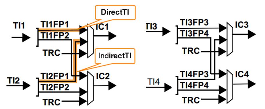
TIM_ICSelection: Input Channel Selection. The signal of the capture channel ICx can come from three input channels, namely TIM_ICSelection_DirectTI, TIM_ICSelection_IndirectTI, or TIM_ICSelection_TRC. The specific differences can be seen in the mapping diagram of input channels and capture channels IC. If it is a normal input capture, all four channels can be used. If it is a PWM input, only channels 1 and 2 can be used. It sets the value of the CCxS[1:0] bits in the CCRx register.
TIM_ICPrescaler: The input capture channel pre-divider can be set to 1x, 2x, 4x or 8x. It sets the values of the ICxPSC[1:0] bits in the CCMRx register. If you need to capture each valid edge of the input signal, setting 1x is sufficient.
TIM_ICFilter: Input capture filter settings are available, with selectable settings ranging from 0x0 to 0x0F. It determines the values of the ICxF[3:0] bits in the CCMRx register. Usually, we do not use the filter, so we set it to 0.
4.3 TIM_BDTRInitTypeDef
The TIM_BDTRInitTypeDef structure is used to set the break and dead zone parameters, and it is specifically for advanced timers. It is used to configure the output state of the channel during the break period and the dead zone time. It is configured using the TIM_BDTRConfig function to complete the parameter configuration. The members of this structure only correspond to the BDTR register. For the specific usage and configuration of the members, please refer to the detailed description of the BDTR register in the manual.
Code Listing: Advanced Timer - 4 Breaker and Dead Zone Initialization Structure
1. TIM_OSSRState: The selection for the off state in the running mode, it sets the value of the OSSR bit in the BDTR register.
2. TIM_OSSIState: The selection for the off state in the idle mode, it sets the value of the OSSI bit in the BDTR register.
3. TIM_LOCKLevel: Locking level configuration, the value of the LOCK[1:0] bits in the BDTR register.
4. TIM_DeadTime: Configuration of the dead zone generator, defining the duration of the dead zone, the selectable range is from 0x0 to 0xFF. It sets the value of the DTG[7:0] bits in the BDTR register.
5. TIM_Break: Selection of the break input function, it can be enabled or disabled. It sets the value of the BKE bit in the BDTR register.
6. TIM_BreakPolarity: Selection of the polarity of the break input channel BRK, it can be high-level valid or low-level valid. It sets the value of the BKP bit in the BDTR register.
- TIM_AutomaticOutput: Automatic output enable, it can be enabled or disabled, it sets the value of the AOE bit in the BDTR register.
WIZnet is a fabless semiconductor company founded in 1998. Its products include the Internet processor iMCU™, which utilizes TOE (TCP/IP Offload Engine) technology and is based on a unique patented fully hardwired TCP/IP. The iMCU™ is designed for embedded Internet devices in various applications.
WIZnet has more than 70 distributors globally and has offices in Hong Kong, South Korea, and the United States, providing technical support and product marketing services.
The regions managed by the Hong Kong office include Australia, India, Turkey, and Asia (excluding South Korea and Japan).