
Chapter 21: W55MH32’s TIM - General Timer
Chapter 21: W55MH32’s TIM - General Timer
Chapter 21: W55MH32’s TIM - General Timer
1Introduction to the Timer
The general timer is composed of a 16-bit auto-load counter driven by a programmable prescaler. It is applicable in various scenarios, such as measuring the pulse length of input signals (input capture) or generating output waveforms (output comparison and PWM). By using the timer prescaler and the RCC clock controller prescaler, the pulse length and waveform period can be adjusted within several microseconds to several milliseconds. Each timer is completely independent and does not share any resources with each other. They can operate synchronously together.
2. Main functions of the general timer
Main function
The general TIMx (TIM2, TIM3, TIM4 and TIM5) timer functions include:
● 16-bit up, down, up/down auto-load counter
● 16-bit programmable (can be modified in real time) prescaler, the frequency division coefficient of the counter clock is any value between 1 and 65536
● 4 independent channels:
〇 Input capture
〇 Output comparison
〇 PWM generation (edge or middle-aligned mode)
〇 Single pulse mode output
● Synchronization circuit for controlling the timer and inter-timer connection using external signals
● Interrupt/DMA is generated when the following events occur:
〇 Update: counter overflows up/down, counter initialization (through software or internal/external trigger)
〇 Trigger event (counter starts, stops, initializes or is triggered by internal/external)
〇 Input capture
〇 Output comparison
● Supports incremental (orthogonal) encoder and Hall sensor circuits for positioning
● Trigger input as an external clock or for periodic current management
The general timer function block diagram is as follows:
3 General Timer Function Description
3.1 Time Base Unit
The main component of the programmable universal timer is a 16-bit counter and an associated auto-load register. This counter can count upwards, downwards, or both upwards and downwards. The clock of this counter is obtained by dividing the pre-divider.
The counter, the automatic loading register and the pre-divider register can be read and written by software, and they can still be read and written while the counter is running. The timing unit includes:
● Counter register (TIMx_CNT)
● Prescaler register (TIMx_PSC)
● Auto-reload register (TIMx_ARR)
The automatic loading registers are pre-loaded. Writing or reading the automatic reloading registers will access the pre-loaded registers. Depending on the setting of the automatic loading pre-load enable bit (ARPE) in the TIMx_CR1 register, the contents of the pre-loaded registers are immediately transferred or sent to the shadow registers at each update event UEV. When the counter reaches the overflow condition (the underflow condition when counting downwards) and when the UDIS bit in the TIMx_CR1 register is equal to '0', an update event is generated. The update event can also be generated by software. The generation of the update event in each configuration will be described in detail later.
The counter is driven by the clock output CK_CNT of the prescaler. CK_CNT is valid only when the counter enable bit (CEN) in the TIMx_CR1 register is set.
Note: The actual counter enable signal CNT_EN is set one clock cycle after CEN.
Description of Pre-Divider
The prescaler can divide the clock frequency of the counter by any value between 1 and 65536. It is a 16-bit counter controlled by a 16-bit register (in the TIMx_PSC register). This control register has a buffer, which can be changed while it is in operation. The new prescaler parameters are adopted when the next update event occurs, providing an example of changing the counter parameters during the operation of the prescaler. When the prescaler parameters change from 1 to 2, the timing diagram of the counter is as follows:
When the parameters of the pre-divider change from 1 to 4, the timing diagram of the counter is as follows:
3.2 Counter mode
Ascending count mode
In the upward counting mode, the counter starts counting from 0 to the automatically loaded value (the content of TIMx_ARR counter), and then restarts from 0 and generates a counter overflow event.
An update event can be generated each time the counter overflows. This can also be achieved by setting the UG bit in the TIMx_EGR register (either through software or using the mode controller). Setting the UDIS bit in the TIMx_CR1 register can disable the update event; this avoids updating the shadow register when writing a new value into the preload register. No update event will be generated until the UDIS bit is cleared to '0'. However, when an update event should occur, the counter will still be reset to 0, and the counter of the prescaler will also be reset (but the prescaler coefficient remains unchanged). Additionally, if the URS bit is set in the TIMx_CR1 register (selecting the update request), setting the UG bit will generate an update event UEV, but the hardware will not set the UIF flag (i.e., no interrupt or DMA request will be generated); this is to avoid generating both update and capture interrupts when clearing the counter in capture mode.
When an update event occurs, all registers are updated, and the hardware simultaneously (depending on the URS bit) sets the update flag (the UIF bit in the TIMx_SR register).
The buffer of the prescaler is set with the value loaded into the preloading register (the content of the TIMx_PSC register).
The automatic loading of the shadow register is re-set with the value of the preloading register (TIMx_ARR).
The following figure provides some examples of the actions of the counter under different clock frequencies when TIMx_ARR = 0x36. When the internal clock prescaler factor is 1, the counter timing diagram is:
Internal clock division factor is 2. Counter timing diagram:
The internal clock division factor is 4. The counter timing diagram is:
Internal clock division factor is N. Counter timing diagram:
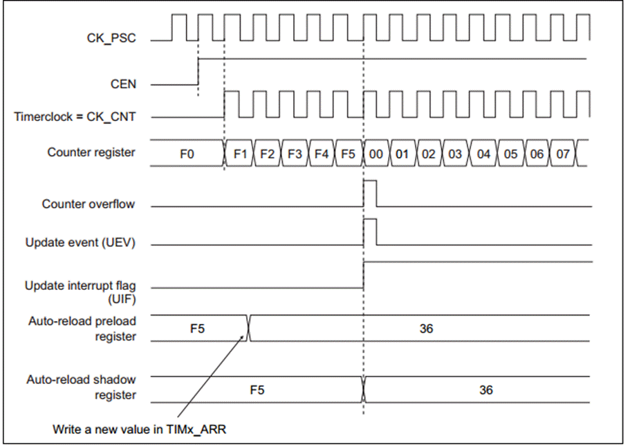
When ARPE = 0 (the update event TIMx_ARR is not preloaded), the counter timing diagram:
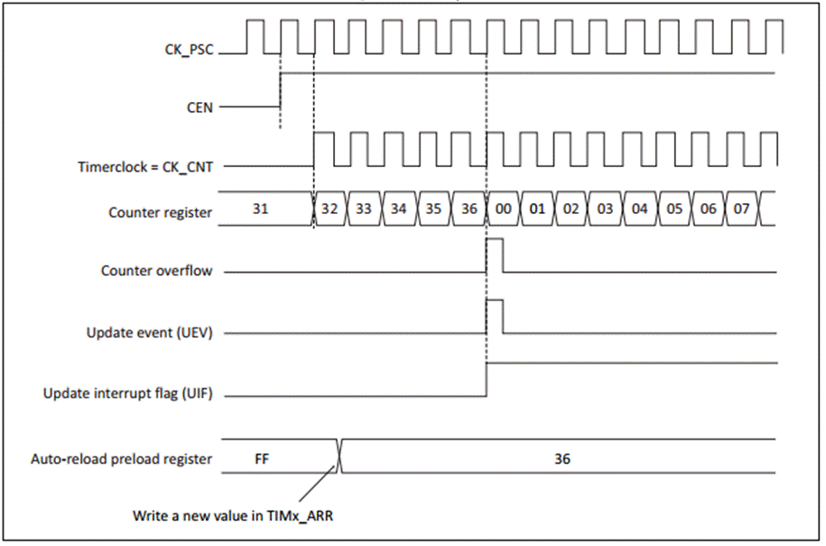
The update event when ARPE = 1 (with TIMx_ARR preloaded): Counter timing diagram:
3.3 Capture/Comparison Channel
Each capture/comparison channel is centered around a capture/comparison register (including a shadow register), including the capture input section (digital filtering, multiplexing, and pre-divider) and the output section (comparator and output control). The following figures provide an overview of a capture/comparison channel.
The input section samples the corresponding TIx input signal and generates a filtered signal TIxF. Then, an edge detector with polarity selection generates a signal (TIxFPx), which can be used as an input trigger from the mode controller or as capture control. This signal passes through a pre-divider and enters the capture register (ICxPS):
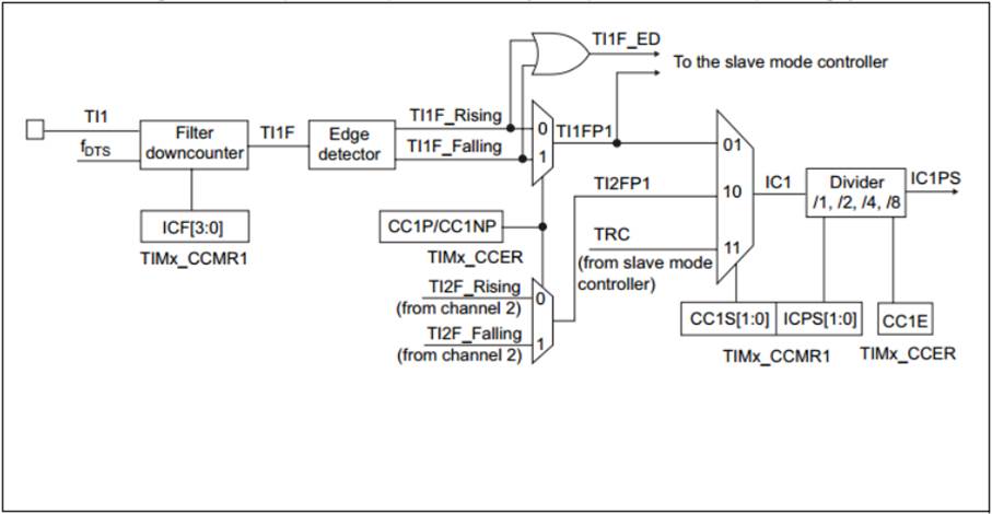
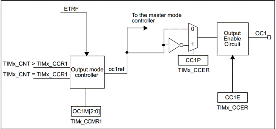
The output section generates an intermediate waveform OCxRef (high active) as the reference, and the end of the chain determines the polarity of the final output signal.
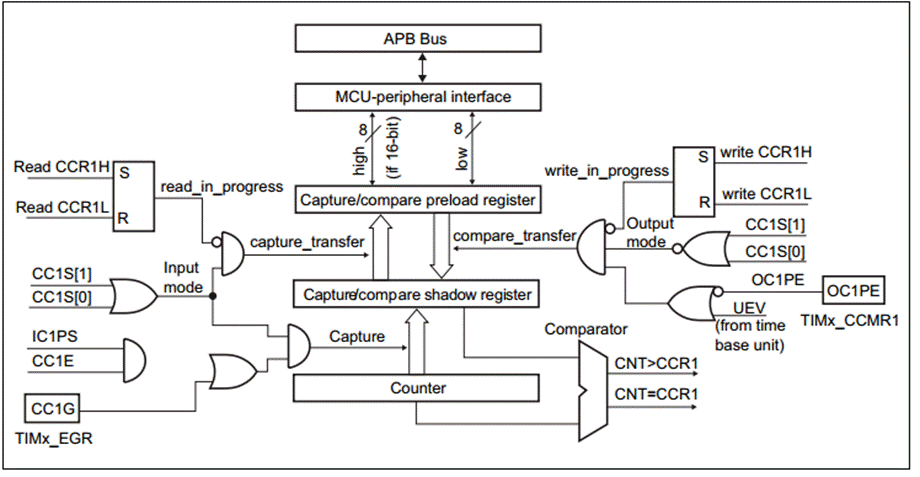
Capture/Compare Channel 1 Main Circuit
The capture/comparison module consists of a pre-loaded register and a shadow register. The read-write process only operates on the pre-loaded register.
In the capture mode, the capture occurs on the shadow register, and then it is copied to the pre-loaded register.
In the comparison mode, the content of the pre-loaded register is copied to the shadow register, and then the content of the shadow register is compared with the counter.
3.4 Input Capture Mode
Based on the characteristics of the input signal, configure the input filter to the required bandwidth (that is, when the input is TIx, the control bit of the input filter is the ICxF bit in the TIMx_CCMRx register). Assuming that the input signal fluctuates within a maximum of 5 internal clock cycles, we must configure the filter's bandwidth to be longer than 5 clock cycles. Therefore, we can (at the fDTS frequency) sample 8 times to confirm a real edge transition on TI1, that is, write IC1F=0011 in the TIMx_CCMR1 register.
Select the valid transition edge of the TI1 channel and write CC1P=0 (rising edge) in the TIMx_CCER register.
Configure the input prescaler. In this case, we want to capture the event at each valid level transition, so the prescaler is disabled (write IC1PS=00 in the TIMx_CCMR1 register).
Set TIMx_CCER register's CC1E=1 to allow the capture value of the counter to be stored in the capture register.
If necessary, enable the related interrupt request by setting the CC1IE bit in the TIMx_DIER register, and enable the DMA request by setting the CC1DE bit in the TIMx_DIER register.
When an input capture occurs:
When an effective level transition occurs, the value of the counter is transmitted to the TIMx_CCR1 register.
The CC1IF flag is set (interrupt flag). When at least 2 consecutive captures occur and CC1IF has not been cleared, CC1OF is also set to '1'.
If the CC1IE bit is set, an interrupt will be generated.
If the CC1DE bit is set, a DMA request will also be generated.
To handle capture overflow, it is recommended to read the data before reading the capture overflow flag, in order to avoid losing the capture overflow information that may be generated after reading the capture overflow flag and before reading the data.
Note: Set the corresponding CCxG bit in the TIMx_EGR register to generate an input capture interrupt and/or DMA request through software.
3.5 PWM Input Mode (Applicable only to TIM9/12)
This mode is a special case of the input capture mode. Apart from the following differences, the operation is the same as that of the input capture mode:
Two ICx signals are mapped to the same TIx input.
These two ICx signals are edge-triggered, but with opposite polarities.
One TIxFP signal is used as the trigger input signal, and the mode controller is configured as the reset mode.
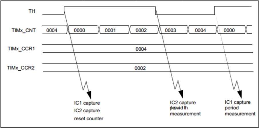
For example, you need to measure the length (TIMx_CCR1 register) and duty cycle (TIMx_CCR2 register) of the PWM signal input to TI1. The specific steps are as follows (depending on the frequency of CK_INT and the value of the prescaler):
Select the valid input of TIMx_CCR1: Set the TIMx_CCMR1 register's CC1S = 01 (select TI1).
Select the valid polarity of TI1FP1 (used to capture data into TIMx_CCR1 and clear the counter): Set CC1P = 0 (rising edge triggered).
Select the valid input of TIMx_CCR2: Set the TIMx_CCMR1 register's CC2S = 10 (select TI1).
Select the valid polarity of TI1FP2 (to capture data into TIMx_CCR2): Set CC2P = 1 (falling edge triggered).
Select the valid trigger input signal: Set the TIMx_SMCR register's TS = 101 (select TI1FP1).
Configure the mode controller as the reset mode: Set TIMx_SMCR's SMS = 100.
Enable capture: Set the TIMx_CCER register's CC1E = 1 and CC2E = 1.
The timing sequence for PWM input mode is as follows:
3.6 Output Comparison Mode
This function is used to control an output waveform or to indicate that a given period of time has elapsed. When the counter matches the content of the capture/comparison register, the output comparison function performs the following operations:
The values defined by the output comparison mode (OCxM bit in TIMx_CCMRx register) and the output polarity (CCxP bit in TIMx_CCER register) are output to the corresponding pins. When a match occurs, the output pin can maintain its level (OCxM = 000), be set to an active level (OCxM = 001), be set to an inactive level (OCxM = 010), or be inverted (OCxM = 011).
The flag in the interrupt status register (CCxIF bit in TIMx_SR register) is set.
If the corresponding interrupt mask (CCxIE bit in TIMx_DIER register) is set, an interrupt is generated.
If the corresponding enable bit (CCDE bit in TIMx_DIER register and CCDS bit in TIMx_CR2 register) is set, a DMA request is generated.
The OCxPE bit in TIMx_CCMRx selects whether the TIMx_CCRx register needs to use the preloading register. In the output comparison mode, the update event UEV has no effect on OCxREF and OCx output.
The synchronization accuracy can reach one counting cycle of the counter. The output comparison mode (in single pulse mode) can also be used to output a single pulse.
Configuration steps for the output comparison mode:
1. Select the counter clock (internal, external, prescaler)
2. Write the corresponding data into the TIMx_ARR and TIMx_CCRx registers
3. If an interrupt request and/or a DMA request is to be generated, set the CCxIE bit and/or the CCxDE bit.
4. Select the output mode, for example, when the counter CNT matches CCRx, the output pin of OCx is toggled. CCRx is preloaded unused, turn on the output of OCx and make it active high. Then, the OCxM should be '011', OCxPE should be '0', CCxP should be '0', and CCxE should be '1'.
5. Set the CEN bit in the TIMx_CR1 register to start the counter
The TIMx_CCRx register can be updated via software at any time to control the output waveform, provided that the preloaded register is not used (OCxPE = '0'; otherwise, the shadow register TIMx_CCRx can only be updated when the next update event occurs). The following figure provides an example.
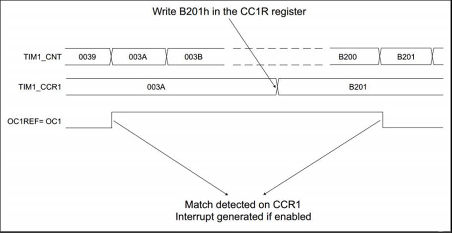
Output comparison mode, invert OC1
3.7 PWM Mode
The pulse width modulation mode can generate a signal whose frequency is determined by the TIMx_ARR register and whose duty cycle is determined by the TIMx_CCRx register.
By writing '110' (PWM mode 1) or '111' (PWM mode 2) to the OCxM bit in the TIMx_CCMRx register, each OCx output channel can independently generate one PWM signal. The OCxPE bit in the TIMx_CCMRx register must be set to enable the corresponding preload register. Finally, the ARPE bit in the TIMx_CR1 register (in up-counting or symmetric mode) must be set to enable the automatically reloaded preload register.
Only when an update event occurs, can the pre-loaded registers be transferred to the shadow registers. Therefore, before the counter starts counting, all the registers must be initialized by setting the UG bit in the TIMx_EGR register. The polarity of OCx can be set through software in the TIMx_CCER register using the CCxP bit, which can be set to be high-level effective or low-level effective. The CCxE bit in the TIMx_CCER register controls the enable of OCx output. Refer to the description of the TIMx_CCERx register for details.
In PWM mode (mode 1 or mode 2), TIMx_CNT and TIMx_CCRx are always compared (depending on the counting direction of the counter) to determine whether TIMx_CCRx ≤ TIMx_CNT or TIMx_CNT ≤ TIMx_CCRx. However, to be consistent with the function of OCREF_CLR (an external event on the ETR signal can clear OCxREF before the next PWM cycle), the OCxREF signal can only be generated under the following conditions:
When the comparison result changes
When the output comparison mode (the OCxM bit in the TIMx_CCMRx register) switches from "freezing" (no comparison, OCxM='000') to a certain PWM mode (OCxM='110' or '111'). Thus, the PWM output can be forcibly set through software during operation.
Depending on the status of the CMS bit in the TIMx_CR1 register, the timer can generate edge-aligned PWM signals or center-aligned PWM signals.
PWM edge alignment mode
Upward counting configuration
When the DIR bit in the TIMx_CR1 register is at a low level, the upward counting is executed.
Here is an example of PWM mode 1. When TIMx_CNT < TIMx_CCRx, the PWM signal reference OCxREF is high, otherwise it is low. If the comparison value in TIMx_CCRx is greater than the auto-reload value (TIMx_ARR), then OCxREF remains at '1'.
If the comparison value is 0, then OCxREF remains at '0'. The following figure shows an example of the PWM waveform with edge alignment when TIMx_ARR = 8.
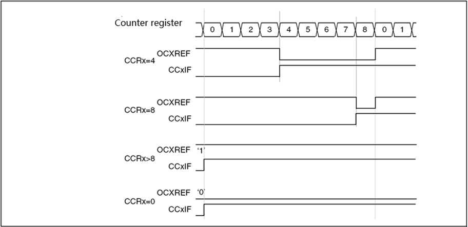
Edge-aligned PWM waveform (ARR = 8)
The configuration for counting downwards
When the DIR bit in the TIMx_CR1 register is at a high level, the decrementing operation is performed. In PWM mode 1, when TIMx_CNT > TIMx_CCRx, the reference signal OCxREF is low; otherwise, it is high. If the comparison value in TIMx_CCRx is greater than the auto-reload value in TIMx_ARR, then OCxREF remains at '1'. In this mode, a 0% PWM waveform cannot be generated.
PWM Center Alignment Mode
When the CMS bit in the TIMx_CR1 register is not '00', it is in the center-aligned mode (all other configurations have the same effect on the OCxREF/OCx signals). Depending on the different CMS bit settings, the compare flag can be set '1' when the counter is counting upwards, when it is counting downwards, or when it is counting both upwards and downwards. The count direction bit (DIR) in the TIMx_CR1 register is updated by hardware and should not be modified by software.
The following figure provides some examples of central-aligned PWM waveforms.
TIMx_ARR=8
PWM Mode 1
In the CMS=01 setting of the TIMx_CR1 register, the compare flag is set when the counter counts down in Central Alignment Mode
Hint for using the center alignment mode:
When entering the center alignment mode, use the current upward/downward counting configuration; this means that whether the counter counts upward or downward depends on the current value of the DIR bit in the TIMx_CR1 register. Additionally, the software cannot simultaneously modify the DIR and CMS bits.
It is not recommended to rewrite the counter while running in the center alignment mode, as this can result in unpredictable outcomes. Specifically: If the value written to the counter is greater than the auto-reload value (TIMx_CNT > TIMx_ARR), the direction will not be updated. For example, if the counter is counting upward, it will continue to do so. If 0 or the value of TIMx_ARR is written to the counter, the direction is updated, but no update event UEV is generated.
The safest way to use the center alignment mode is to generate a software update (set the UG bit in TIMx_EGR) before starting the counter, and do not modify the counter's value during the counting process.
4 PWM
4.1 Code analysis
1.Header file inclusion and global variable definition
#include <stdlib.h>Header file: Standard library header files and custom header files are introduced. delay.h may be used for delay functionality, and w55mh32.h may contain hardware-related definitions.
Global variable: USART_TEST is a pointer of type USART_TypeDef and is initialized as USART1, used for subsequent serial port operations.
2. Function Declaration
void UART_Configuration(uint32_t bound);Three functions are declared:
UART_Configuration: used for configuring serial communication.
TIM_Configuration: used for configuring the timer and generating PWM signals.
RCC_ClkConfiguration: used for configuring the system clock.
3. Main function
RCC_ClocksTypeDef clocks;System initialization:
Call the RCC_ClkConfiguration function to configure the system clock.
Call the delay_init function to initialize the delay functionality.
Call the UART_Configuration function to configure the serial communication, with the baud rate set to 115200.
Call the RCC_GetClocksFreq function to obtain the system clock frequency information.
Output information:
Use the printf function to output the system clock frequency information, including the system clock (SYSCLK), high-performance bus clock (HCLK), low-speed peripheral bus clock (PCLK1), high-speed peripheral bus clock (PCLK2), and ADC clock (ADCCLK).
Output prompt information "TIM Out Test.", indicating the start of the timer output test.
Timer configuration:
Call the TIM_Configuration function to configure the timer and output the PWM signal.
Main loop: while (1); It is an infinite loop that causes the program to stop here and wait for the timer to output the PWM signal.
4. RCC_ClkConfiguration Function
void RCC_ClkConfiguration(void)Clock reset:
Call the RCC_DeInit function to reset the RCC registers to their default values.
External high-speed clock (HSE) configuration: Call the RCC_HSEConfig function to enable the external high-speed clock (HSE).
Wait for the HSE to be ready (set the RCC_FLAG_HSERDY flag).
PLL configuration:
Call the RCC_PLLCmd function to disable the PLL.
Call the RCC_PLLConfig function to configure the PLL, using the HSE as the input clock source, and set the PLL multiplication factor to 9.
Call the RCC_PLLCmd function to enable the PLL.
Wait for the PLL to be ready (set the RCC_FLAG_PLLRDY flag) through a while loop.
System clock configuration:
Call the RCC_SYSCLKConfig function to use the PLL output as the system clock.
Bus clock configuration:
Call the RCC_HCLKConfig function to directly use the system clock (SYSCLK) as the high-performance bus clock (HCLK).
Call the RCC_PCLK1Config function to divide HCLK by 2 as the low-speed peripheral bus clock (PCLK1).
Call the RCC_PCLK2Config function to directly use HCLK as the high-speed peripheral bus clock (PCLK2).
Low-speed internal clock (LSI) and high-speed internal clock (HSI) configuration:
Call the RCC_LSICmd function to enable the low-speed internal clock (LSI), and wait for LSI to be ready (set the RCC_FLAG_LSIRDY flag).
Call the RCC_HSICmd function to enable the high-speed internal clock (HSI), and wait for HSI to be ready (set the RCC_FLAG_HSIRDY flag).
5. TIM_Configuration Function
void TIM_Configuration(void)
Clock Enable:
Call the RCC_APB1PeriphClockCmd function to enable the clock of Timer 3 (TIM3).
Call the RCC_APB2PeriphClockCmd function to enable the clocks of GPIOA and AFIO (re-mapping function module).
GPIO Configuration:
Configure GPIOA's Pin 7 as a re-mapped push-pull output mode for outputting the PWM signal of TIM3's channel 2 (TIM_CH2).
Set the GPIO speed to 50MHz.
Basic Parameters Configuration of Timer:
Define the TIM_TimeBaseInitTypeDef structure type for configuring the basic parameters of the timer.
Set TIM_Period to 99, representing the automatic reload value of the timer.
Set TIM_Prescaler according to the PCLK1 frequency, dividing the timer's clock frequency.
Set TIM_ClockDivision to TIM_CKD_DIV1, indicating a clock division factor of 1.
Set TIM_CounterMode to TIM_CounterMode_Up, indicating that the timer uses an upward counting mode.
Call the TIM_TimeBaseInit function to initialize TIM3 according to the above parameters.
Output Comparison (PWM) Configuration of Timer:
Define the TIM_OCInitTypeDef structure type for configuring the output comparison (PWM) parameters of the timer.
Set TIM_OCMode to TIM_OCMode_PWM2, indicating the use of PWM mode 2.
Set both TIM_OutputState and TIM_OutputNState to TIM_OutputState_Enable, indicating enabling the output and complementary output.
Set TIM_Pulse to 99 / 2, indicating the pulse width of the PWM signal.
Set TIM_OCPolarity and TIM_OCNPolarity to TIM_OCPolarity_Low, indicating the output polarity as low.
Set TIM_OCIdleState to TIM_OCIdleState_Set and TIM_OCNIdleState to TIM_OCIdleState_Reset, indicating the output level in the idle state.
Call the TIM_OC2Init function to initialize TIM3's channel 2 according to the above parameters.
Preload Register Configuration:
Call the TIM_OC2PreloadConfig function to enable the preload register of TIM3 channel 2.
Call the TIM_ARRPreloadConfig function to enable the preload function of the automatic reload register of TIM3.
Timer Enable:
Call the TIM_Cmd function to enable TIM3.
Call the TIM_CtrlPWMOutputs function to enable the PWM output of the advanced timer.
5. UART_Configuration Function
void UART_Configuration(uint32_t bound)Clock Enable:
Call the RCC_APB2PeriphClockCmd function to enable the clocks for USART1 and GPIOA.
GPIO Configuration:
Configure GPIOA's Pin 9 as a re-mapped push-pull output mode for the USART1's transmission function.
Configure GPIOA's Pin 10 as an open-drain input mode for the USART1's reception function.
Set the GPIO speed to 50MHz.
USART Configuration:
Define the USART_InitStructure structure of type USART_InitTypeDef to configure the basic parameters of USART.
Set USART_BaudRate according to the passed parameter bound to set the baud rate.
Set USART_WordLength to USART_WordLength_8b, indicating that the data bits are 8 bits.
Set USART_StopBits to USART_StopBits_1, indicating that the stop bit is 1 bit.
Set USART_Parity to USART_Parity_No, indicating no parity bit.
Set USART_HardwareFlowControl to USART_HardwareFlowControl_None, indicating no hardware flow control.
Set USART_Mode to USART_Mode_Rx | USART_Mode_Tx, indicating support for receive and transmit modes.
Call the USART_Init function to initialize USART1 according to the above parameters.
Call the USART_Cmd function to enable USART1.
7. SER_PutChar and fputc functions
int SER_PutChar(int ch)The SER_PutChar function is used to send a character to the serial port. The USART_GetFlagStatus function is used to check the serial port transmission completion flag. After the transmission is completed, the USART_SendData function is called to send the character.
The fputc function redirects the output of the printf function and sends the characters through the serial port. When a newline character '\n' is encountered, it first calls the SER_PutChar('\r') function to send the carriage return character '\r'.
4.2 Download Verification
If you want to check the duty cycle of the PWM output, you can add this code to the loop.
This can be used to print out the duty cycle of the PWM.
5. Update Interruption
5.1 Code Analysis
1. Main function: Initialization and startup
int main(void) {2. UART_Configuration: Serial Port Initialization
void UART_Configuration(uint32_t bound) {3. TIM_Configuration: Configuration of Timer TIM3
4. Interrupt handling function: TIM3_IRQHandler
void TIM3_IRQHandler(void) {This code demonstrates the basic usage of the W55MH32 timer: configuring the update interrupt of TIM3, triggering periodically and outputting information via the serial port. The core process: timer initialization (prescaler, period) → enabling interrupts → interrupt handling (printing information). It is suitable for scenarios requiring periodic tasks (such as periodic sampling, heartbeat signals).
5.2 Download Verification
6 TIM_CalibrationLsi
6.1 Code Analysis
1. Global variable
uint8_t TIM5_CAPTURE_STA = 0; 2. Main function: Initialization and main loop
int main(void) {3. TIM_Configuration: Timer Input Capture Configuration
void TIM_Configuration(void) {4. Interrupt handler:TIM5_IRQHandler
void TIM5_IRQHandler(void) {5. System Clock Configuration: RCC_ClkConfiguration
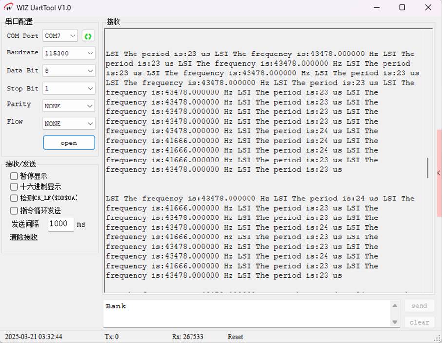
void RCC_ClkConfiguration(void) {This code is a typical example of the advanced application of the W55MH32 timer, demonstrating how to utilize the hardware features to measure internal signals. It is suitable for embedded system debugging and clock calibration scenarios.
6.2 Download Verification
7 TIM_InputCapture
7.1 Code Analysis
1.Global variable
uint8_t TIM3_CAPTURE_STA = 0; 2. Main function: Initialization and main loop
int main(void) {3. TIM_Configuration: Timer Input Capture Configuration
void TIM_Configuration(void) {4. Interrupt handling function:TIM3_IRQHandler
void TIM3_IRQHandler(void) {5. System Clock Configuration
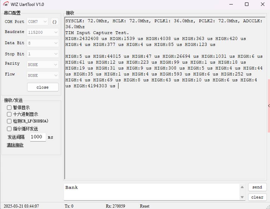
void RCC_ClkConfiguration(void) {This code is a typical application of the W55MH32 timer input capture, demonstrating how to efficiently measure external signals through hardware interrupts. It is suitable for embedded systems that require high-precision time measurement.
7.2 Download Verification
8 TIM_Tim9
8.1 Code Analysis
1.Header file and global variables
#include "w55mh32.h" 2. Main function: Initialization and startup
int main(void) {3. UART_Configuration: Serial Port Initialization
void UART_Configuration(uint32_t bound) {4. TIM_Configuration: Configuration of Timer TIM9
void TIM_Configuration(void) {5. Interrupt handling function: TIM1_BRK_TIM9_IRQHandler
void TIM1_BRK_TIM9_IRQHandler(void) {6. printf redirection: Serial port output
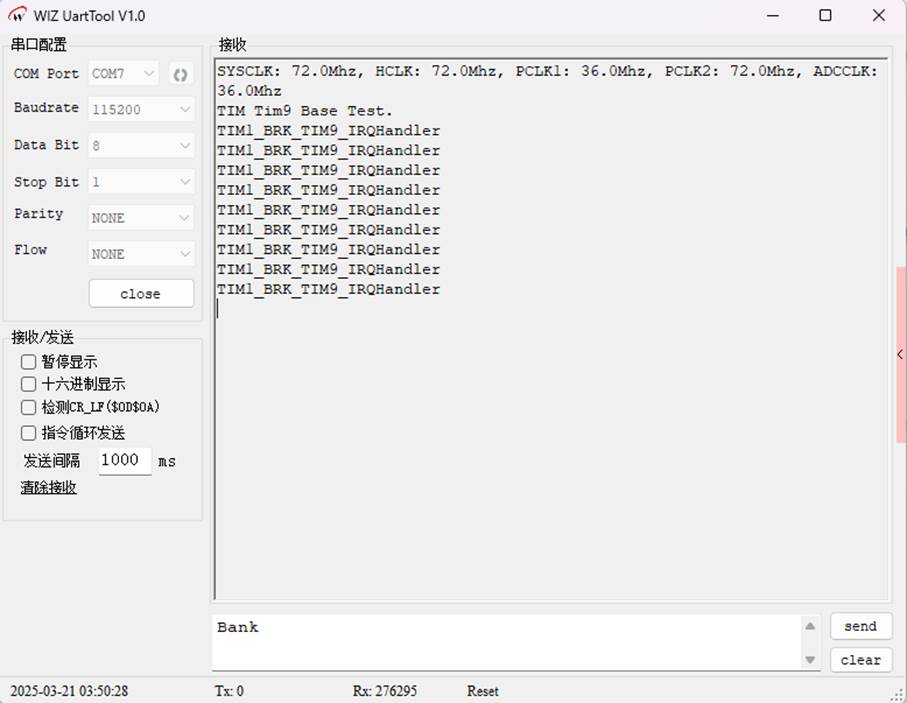
int fputc(int c, FILE *f) {This code demonstrates the basic usage of the W55MH32 timer TIM9: configuring for update interrupts, triggering periodically and outputting information via serial port. The core process: timer initialization (prescaler, period) → enabling interrupts → interrupt handling (printing information). It is suitable for scenarios requiring periodic tasks (such as periodic sampling, heartbeat signals).
8.2 Download Verification
WIZnet is a fabless semiconductor company founded in 1998. Its products include the Internet processor iMCU™, which utilizes TOE (TCP/IP Offload Engine) technology and is based on a unique patented fully hardwired TCP/IP. The iMCU™ is designed for embedded Internet devices in various applications.
WIZnet has more than 70 distributors globally and has offices in Hong Kong, South Korea, and the United States, providing technical support and product marketing services.
The regions managed by the Hong Kong office include Australia, India, Turkey, and Asia (excluding South Korea and Japan).