
Chapter 18: W55MH32’s I2C Communication Test
Chapter 18: W55MH32’s I2C Communication Test
Chapter 18: W55MH32’s I2C Communication Test
References for this chapter: "W55MH32 Reference Manual" - I2C section and "I2C Bus Protocol".
If you are not familiar with the I2C communication protocol, you can first read the content of the "I2C Bus Protocol" document to learn about it.
1 Introduction to I2C Protocol
The I2C communication protocol (Inter-Integrated Circuit) was developed by Philips. Due to its few pins, simple hardware implementation, strong scalability, and the fact that it does not require external transceiver devices such as USART or CAN for communication, it is now widely used for communication between multiple integrated circuits (ICs) within a system.
In computer science, most complex problems can be simplified through layering. For example, chips are divided into the core layer and on-chip peripherals; the W55MH32 standard library is a software layer between registers and user code. For communication protocols, we also understand them through layering. The most basic division is to classify them into the physical layer and the protocol layer. The physical layer specifies the characteristics of the mechanical and electronic components in the communication system, ensuring the transmission of raw data over the physical medium. The protocol layer mainly defines the communication logic and standardizes the data packaging and unpacking between the sender and receiver.
Now, let's explain the physical layer and protocol layer of the I2C protocol separately.
1.1 I2C Physical Layer
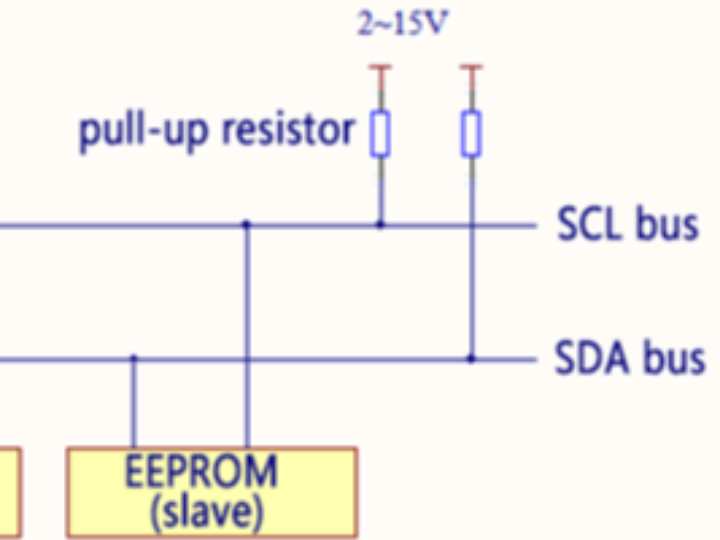
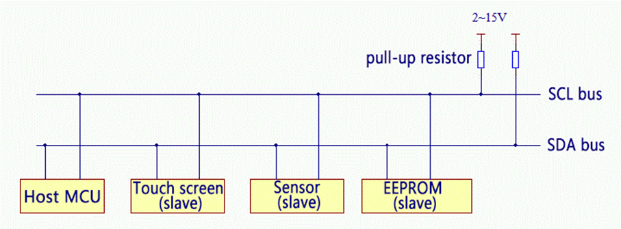
The common connection methods between I2C communication devices are shown in the following figure. Common I2C communication systems:
Its physical layer has the following characteristics:
1. It is a bus that supports devices. "Bus" refers to the common signal lines shared by multiple devices. In an I2C communication bus, multiple I2C communication devices can be connected, and multiple communication hosts and multiple communication slaves can be supported.
2. An I2C bus only uses two bus lines, one bidirectional serial data line (SDA) and one serial clock line (SCL). The data line is used to represent data, and the clock line is used for data transmission synchronization.
3. Each device connected to the bus has an independent address. The host can use this address to access different devices.
4. The bus is connected to the power supply through an upper pull-up resistor. When an I2C device is idle, it outputs a high-impedance state, and when all devices are idle, all output high-impedance states, and the upper pull-up resistor pulls the bus to a high level.
5. When multiple hosts use the bus simultaneously, to prevent data conflicts, arbitration is used to determine which device occupies the bus.
6. There are three transmission modes: the standard mode has a transmission rate of 100 kbit/s, the fast mode has a transmission rate of 400 kbit/s, and the high-speed mode can reach 3.4 Mbit/s. However, most I2C devices currently do not support the high-speed mode.
7. The number of ICs connected to the same bus is limited by the maximum capacitance of the bus, which is 400 pF.
1.2 Protocol Layer
The I2C protocol defines the initiation and termination signals for communication, data validity, responses, arbitration, clock synchronization, and address broadcasting, among other aspects.
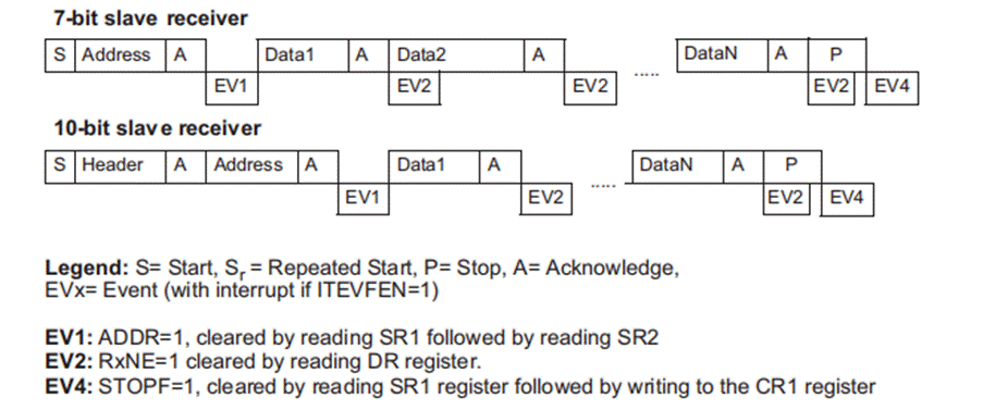
1.2.1 Basic I2C Read-Write Process
Let's first take a look at the basic structure of the I2C communication process. The communication process is shown in the following figure. The host writes data to the slave device, and the host reads data from the slave device. And the I2C communication composite format is
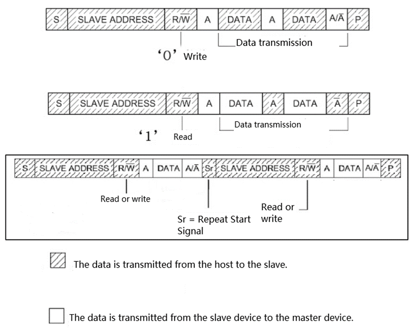
These diagrams represent the sequence of data packets on the SDA line during communication between the host and the slave.
Here, S stands for the transmission start signal (S) generated by the I2C interface of the host. At this time, all slaves connected to the I2C bus will receive this signal.
After the start signal is generated, all slaves start to wait for the slave address signal (SLAVE_ADDRESS) that the host broadcasts next. On the I2C bus, each device's address is unique. When the address broadcast by the host matches the address of a certain device, that device is selected, and the unselected devices will ignore the subsequent data signals. According to the I2C protocol, this slave address can be 7 bits or 10 bits.
After the address bits, there is a transmission direction selection bit. When this bit is 0, it indicates that the subsequent data transmission direction is from the host to the slave, that is, the host writes data to the slave. When this bit is 1, it is the opposite, that is, the host reads data from the slave.
After the slave receives the matching address, either the host or the slave will return an acknowledge (ACK) or non-acknowledge (NACK) signal. Only after receiving the acknowledge signal can the host continue to send or receive data.
Write data
If the direction transmission bit is set to "write data" (as in the first figure), after broadcasting the address and receiving the response signal, the host begins to officially transmit data (DATA) to the slave. The size of the data packet is 8 bits. After the host sends one byte of data, it must wait for the response signal (ACK) from the slave. Repeat this process, and the host can transmit N pieces of data to the slave. The value of N has no limit. When the data transmission is completed, the host sends a stop transmission signal (P) to the slave, indicating that it will no longer transmit data.
Read data
If the direction transmission bit is set to "read data" (as in the second diagram), after broadcasting the address and receiving the response signal, the slave device starts to return data (DATA) to the master device. The size of the data packet is also 8 bits. After each data is sent by the slave device, it waits for the response signal (ACK) from the master device. This process is repeated, allowing up to N data to be returned. There is no limit to the value of N. When the master device wishes to stop receiving data, it sends a non-response signal (NACK) to the slave device, and the slave device automatically stops the data transmission.
Reading and writing data
Apart from the basic reading and writing, the I2C communication is more commonly in the composite format, as shown in the third picture. This transmission process has two start signals (S). Generally, in the first transmission, the host finds the slave device through the SLAVE_ADDRESS, and then sends a "data" segment. This data is usually used to represent the register or memory address inside the slave device (note the difference from the SLAVE_ADDRESS); in the second transmission, the content of that address is read or written. That is to say, the first communication is to inform the slave device of the address to be read or written, and the second communication is the actual content to be read or written.
The decomposition of each signal in the above communication process is as follows:
1.2.2 Start and Stop Signals for Communication
The start (S) and stop (P) signals mentioned in the previous text are two special states. Refer to the following figure. Start and stop signals. When the SCL line is at a high level, the SDA line switches from a high level to a low level. This situation indicates the start of communication. When the SCL line is at a high level, the SDA line switches from a low level to a high level, indicating the stop of communication. The start and stop signals are generally generated by the host.
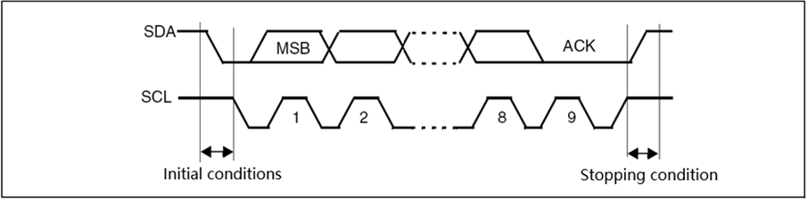
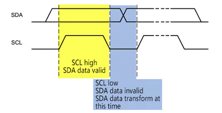
1.2.3 Data Validity
The I2C protocol uses the SDA signal line to transmit data and the SCL signal line for data synchronization. Refer to the following diagram for data validity. The SDA data line transmits one bit of data in each clock cycle of SCL. During transmission, when SCL is at a high level, the data on SDA is valid, that is, when SDA is at a high level, it represents "1" data, and when it is at a low level, it represents "0" data. When SCL is at a low level, the data on SDA is invalid. Usually, at this time, SDA performs a level switch to prepare for the next data representation.
Each data transmission is in units of bytes, and the number of bytes transmitted each time is not restricted.
1.2.4 Address and Data Direction
Each device on the I2C bus has its own independent address. When the host initiates communication, it sends the device address (SLAVE_ADDRESS) through the SDA signal line to locate the slave device. The I2C protocol stipulates that the device address can be 7 bits or 10 bits. In practice, 7-bit addresses are more commonly used. The data bit immediately following the device address is used to indicate the direction of data transmission. It is the data direction bit (R/), the 8th or 11th bit. When the data direction bit is "1", it indicates that the host reads data from the slave device. When this bit is "0", it indicates that the host writes data to the slave device. See the following figure for device addresses and data transmission directions:
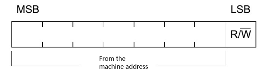
When reading data, the host releases control of the SDA signal line, and the slave controls the SDA signal line. The host receives the signal. When writing data, the SDA is controlled by the host, and the slave receives the signal.
1.2.5 Response
Both data and address transmission in I2C are accompanied by responses. The responses include two signals: "Acknowledge (ACK)" and "Non-Acknowledge (NACK)". As the data receiving end, when a device (whether master or slave) receives a byte of data or address from I2C transmission, if it wants the other party to continue sending data, it needs to send the "Acknowledge (ACK)" signal to the other party. The sender will then continue to send the next data; if the receiving end wants to end the data transmission, it sends the "Non-Acknowledge (NACK)" signal to the other party, and upon receiving this signal, the sender will generate a stop signal to end the signal transmission.
During transmission, the host generates the clock. At the 9th clock, the data sender releases the control of SDA, and the data receiver controls SDA. If SDA is at a high level, it indicates a "Non-Acknowledge (NACK)" signal; if it is at a low level, it indicates an "Acknowledge (ACK)" signal.
The I2C characteristics and architecture of W55MH32
If we directly control the two GPIO pins of W55MH32 and use them as SCL and SDA respectively, following the timing requirements of the aforementioned signals, and directly control the output of the pins (reading the SDA level when receiving data), we can achieve I2C communication. Similarly, if we control the pins according to the requirements of USART, we can also achieve USART communication. Therefore, as long as the protocol is followed, it is standard communication. No matter how you implement it, whether it is a controller produced by ST or a memory produced by ATMEL, they can interact according to the communication standard.
When directly controlling the level of GPIO pins to generate communication timing, it is necessary for the CPU to control the state of the pins at each moment, so this is called the "software simulation protocol" method.
Conversely, there is also the "hardware protocol" method. The I2C on-chip peripheral of W55MH32 is specifically responsible for implementing the I2C communication protocol. As long as the peripheral is configured properly, it will automatically generate communication signals, receive and transmit data, and cache them. The CPU only needs to detect the state of the peripheral and access the data register to complete data transmission. This method of handling the I2C protocol by the hardware peripheral reduces the workload of the CPU and makes the software design simpler.
2.1 Introduction to the I2C Peripheral of W55MH32
The I2C (chip-to-chip) bus interface connects the microcontroller and the serial I2C bus. It provides multi-host functionality, controlling all the specific timings, protocols, arbitration, and timing for the I2C bus. It supports both standard and fast modes, and is compatible with SMBus 2.0. The I2C module has various applications, including the generation and verification of CRC codes, SMBus (System Management Bus) and PMBus (Power Management Bus). Depending on the specific needs of the device, DMA can be used to reduce the burden on the CPU.
2.2 Analysis of the I2C Architecture of W55MH32
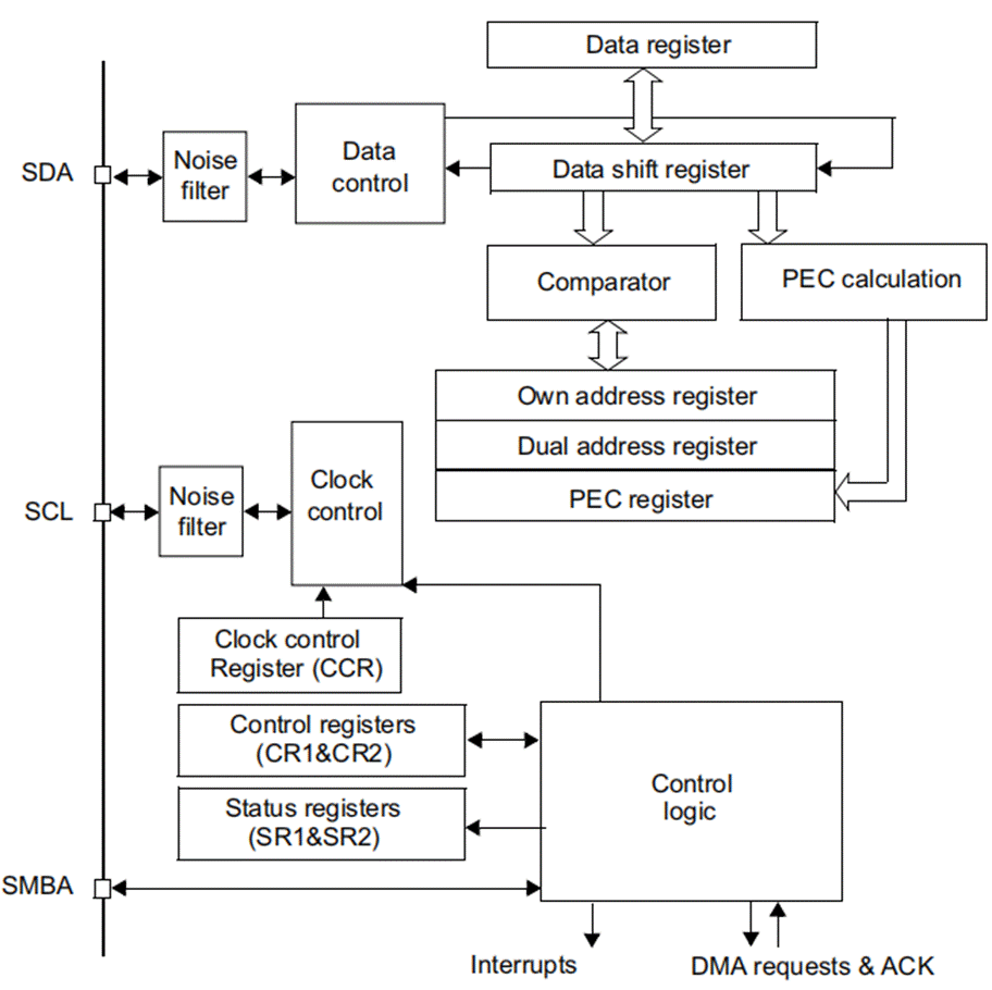
The I2C architecture diagram of W55MH32 is as follows:
2.2.1 Communication Pins
All the hardware architectures of I2C are based on the SCL line and SDA line on the left side of the figure (where the SMBBA line is used for the warning signal of SMBUS, and I2C communication does not use it). The W55MH32 chip has multiple I2C peripherals, and their I2C communication signals are connected to different GPIO pins. When using them, they must be configured to these specified pins. Regarding the reassignment function of GPIO pins, refer to the specification document.
Pin | I2C1 | I2C2 |
SCL | PB6 / PB8 (Re-mapping) | PB10 |
SDA | PB7 / PB9 (Re-mapping) | PB11 |
2.2.2. Clock control logic
The clock signal of the SCL line is controlled by the I2C interface according to the clock control register (CCR). The controlled parameters mainly include the clock frequency. Configuring the CCR register of I2C allows modification of the parameters related to the communication rate:
The "standard/fast" mode of I2C communication can be selected, and these two modes correspond to communication rates of 100/400 Kbit/s for I2C.
In the fast mode, the duty cycle of the SCL clock can be selected, with options of Tlow/Thigh = 2 or Tlow/Thigh = 16/9. We know that the I2C protocol samples the SDA signal when the SCL is at high level, and prepares the next data when the SCL is at low level. Modifying the ratio of the high and low levels of the SCL will affect data sampling, but in fact, the difference in these two modes is not significant. If the requirements are not very strict, you can choose randomly here.
There is also a 12-bit configuration factor CCR in the CCR register, which works together with the input clock source of the I2C peripheral to generate the SCL clock. The I2C peripheral of W55MH32 is all mounted on the APB1 bus, and the clock source used is PCLK1 of APB1. The output clock formula of the SCL signal line is as follows:
Standard Mode:
Thigh=CCR*TPCKL1 Tlow = CCR*TPCLK1
In the rapid mode, when Tlow/Thigh = 2:
Thigh = CCR*TPCKL1 Tlow = 2*CCR*TPCKL1
In the fast mode, when Tlow/Thigh = 16/9:
Thigh = 9*CCR*TPCKL1 Tlow = 16*CCR*TPCKL1
For example, our PCLK1 is 36 MHz. If we want to configure a rate of 400 Kbit/s, the calculation method is as follows:
PCLK clock cycle: TPCLK1 = 1/36,000,000
Target SCL clock cycle: TSCL = 1/400,000
High level time within SCL clock cycle: THIGH = TSCL/3
Low level time within SCL clock cycle: TLOW = 2*TSCL/3
Calculate the value of CCR: CCR = THIGH/TPCLK1 = 30
The result is that CCR is 30. By writing this value to the corresponding register bit, we can control the communication rate of IIC to 400 KHz. Even if the SCL clock configured is not exactly equal to the standard 400 KHz, the correctness of IIC communication will not be affected because all data communication is coordinated by SCL. As long as its clock frequency is not much higher than the standard, it will be fine.
2.2.3. Data Control Logic
The SDA signal of I2C is mainly connected to the data shift register. The data source and destination of the data shift register are the data register (DR), the address register (OAR), the PEC register, and the SDA data line. When sending data outward, the data shift register uses the "data register" as the data source and sends the data bit by bit through the SDA signal line; when receiving data from the outside, the data shift register samples the data on the SDA signal line and stores it bit by bit in the "data register". If data verification is enabled, the received data will be processed by the PCE calculator, and the result will be stored in the "PEC register". When the I2C of W55MH32 operates in the slave mode, when the device address signal is received, the data shift register will compare the received address with the value of its own "I2C address register" to respond to the addressing of the host. The own I2C address of W55MH32 can be modified by modifying the "own address register", and it supports the simultaneous use of two I2C device addresses. The two addresses are stored in OAR1 and OAR2 respectively.
2.2.4. Overall Control Logic
The overall control logic is responsible for coordinating the entire I2C peripheral. The working mode of the control logic changes according to the parameters of the "control registers (CR1/CR2)" we have configured. When the peripheral is operating, the control logic will modify the "status registers (SR1 and SR2)" based on the working status of the peripheral. We can understand the working state of I2C by reading the relevant bits of these registers. In addition, the control logic also, as required, is responsible for controlling the generation of I2C interrupt signals, DMA requests, and various I2C communication signals (start, stop, response signals, etc.).
2.3 Communication Process
When using the I2C peripheral communication, at different stages of the communication, it writes parameters to different data bits of the "status register (SR1 and SR2)". We can understand the communication status by reading the flags of these registers.
2.3.1 Main Transmitter
The communication process of the master transmitter is as shown in the following figure. The figure depicts the "master transmitter" process, that is, when it acts as the host end for I2C communication, the process of sending data outward:
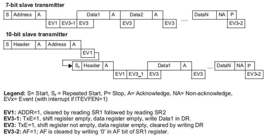
The sending process and event description of the main transmitter are as follows:
The control generates the starting signal (S). Once the starting signal occurs, it generates the event "EV5" and sets the "SB" bit of the SR1 register to 1, indicating that the starting signal has been sent.
Then, the device address is sent and a response signal is awaited. If a slave responds, events "EV6" and "EV8" are generated. At this time, the "ADDR" bit and "TXE" bit of the SR1 register are set to 1, indicating that the address has been sent and the data register is empty.
After the above steps are executed normally and the ADDR bit is cleared, we write the data to be sent to the "data register DR" of the I2C. At this time, the TXE bit is reset to 0, indicating that the data register is not empty. After the I2C peripheral sends the data bit by bit through the SDA signal line, event "EV8" is generated, that is, the TXE bit is set to 1. This process is repeated to send multiple byte data.
When we complete the data transmission, the control of the I2C device generates a stop signal (P). At this time, event "EV8_2" is generated, and both the TXE bit and the BTF bit of SR1 are set to 1, indicating that the communication has ended.
If we enable I2C interrupts, when all the above events occur, an I2C interrupt signal will be generated, and it will enter the same interrupt service function. After reaching the I2C interrupt service program, the register bits are checked to determine which event it is.
2.3.2. Main receiver
Let's analyze the main receiver process, that is, the process of receiving data from the outside when acting as the host end of the I2C communication. As shown in the figure below, the main receiver process:
The receiving process and event description of the main receiver are as follows:
Similar to the sending process, the starting signal (S) is generated by the host end. After the starting signal is generated, it triggers event "EV5", and sets the "SB" bit of the SR1 register to 1, indicating that the starting signal has been sent.
Then, the device address is sent and a response signal is awaited. If a slave responds, event "EV6" is generated. At this time, the "ADDR" bit of the SR1 register is set to 1, indicating that the address has been sent.
After the slave receives the address, it starts sending data to the host end. When the host receives this data, event "EV7" is generated. The RXNE bit of the SR1 register is set to 1, indicating that the data register is not empty. After reading this register, we can clear the register to empty it for receiving the next data. At this time, we can control the I2C to send an response signal (ACK) or a non-response signal (NACK). If there is a response, the above steps are repeated to receive data. If there is no response, the transmission is stopped.
After sending the non-response signal, the stop signal (P) is generated to end the transmission.
During the sending and receiving process, some events not only indicate the status bits mentioned above, but may also simultaneously indicate status bits such as the host status. Moreover, after reading, the flags need to be cleared. This is quite complex. We can use the W55MH32 standard library functions to directly detect the composite flags of these events to reduce the programming difficulty.
3 Detailed Explanation of I2C Initialization Structure
Like other peripherals, the W55MH32 standard library provides an I2C initialization structure and initialization function to configure the I2C peripheral. The structure and function definitions are located in the library files "w55mh32_i2c.h" and "w55mh32_i2c.c". During programming, we can use or refer to the comments in these two files or the library help documentation. After understanding the initialization structure, we can use the I2C peripheral proficiently. See code listing: I2C-1 :
Code Listing: I2C-1 I2C Initialization Structure
typedef struct {The descriptions of these structure members are as follows, where the text within the parentheses represents the macros corresponding to the parameters as defined in the W55MH32 standard library:
I2C_ClockSpeed
This member sets the transmission rate of I2C. When the initialization function is called, the function will calculate the input value and write the clock factor into the I2C clock control register CCR. The parameter value we input must not exceed 400KHz. In fact, since the CCR register cannot write decimal-type clock factors, the actual frequency of SCL may be lower than the parameter value set by this member. In this case, apart from a slightly slower communication, it will not have any other impact on the standard I2C communication.
I2C_Mode
This member selects the I2C usage method. There are I2C mode (I2C_Mode_I2C) and SMBus master and slave modes (I2C_Mode_SMBusHost, I2C_Mode_SMBusDevice). In this case, there is no need to distinguish the master-slave mode for I2C. Simply set I2C_Mode_I2C.
I2C_DutyCycle
This member setting is the duty cycle of the SCL line clock in I2C. This configuration has two options, which are the ratio of low level time to high level time being 2:1 (I2C_DutyCycle_2) and 16:9 (I2C_DutyCycle_16_9). Actually, the difference in these two modes is not significant. Generally, the requirements are not so strict, so you can choose randomly here.
I2C_OwnAddress1
This member is configured with the own address of the W55MH32 I2C device. Each device connected to the I2C bus must have its own address, and even the host is no exception. The address can be set to 7 bits or 10 bits (determined by the I2C_AcknowledgeAddress member below), as long as it is unique on the I2C bus.
The I2C peripheral of the W55MH32 can use two addresses simultaneously, that is, it can respond to two addresses at the same time. This structure member I2C_OwnAddress1 is configured with the default address stored in the OAR1 register. If you need to set the second address register OAR2, you can use the I2C_OwnAddress2Config() function to configure it. OAR2 does not support 10-bit addresses, only 7-bit ones.
I2C_Ack_Enable
This member is about the I2C response settings. When set to enable, it allows the transmission of response signals. This experiment is configured to enable responses (I2C_Ack_Enable), which is a communication requirement for most devices following the I2C standard. Changing it to disable responses (I2C_Ack_Disable) often leads to communication errors.
I2C_AcknowledgeAddress
This member decides whether the addressing mode of I2C is 7-bit or 10-bit address. This choice needs to be made based on the actual addresses of the devices connected to the I2C bus. The configuration of this member also affects the I2C_OwnAddress1 member. Only when this setting is set to 10-bit mode, will I2C_OwnAddress1 support 10-bit addresses.
After setting the values of these structure members, calling the library function I2C_Init() can write the configuration of the structure to the registers.
4 I2C Communication Test
4.1 Programming Key Points
- The target pins for communication configuration are set to open-drain mode;
- Enable the clock of the I2C peripheral;
- Configure the parameters such as mode, address, rate, etc. of the I2C peripheral and enable the I2C peripheral;
- Write the basic function for I2C byte transmission and reception;
4.2 Code Analysis
1.Header files and macro definitions
#include <stdlib.h>The header files of the standard library, the custom delay library and the hardware-related library were introduced, and the buffer size was defined as 256 bytes.
2. Function Declaration
A series of functions are declared, covering the configuration of UART, NVIC, and I2C, I2C master-slave device testing, data filling, printing, and command acquisition, etc.
3. Global Variables
USART_TypeDef *USART_TEST = USART1;The serial port used for testing was defined as USART1, along with the sending buffer, receiving buffer and receiving flag.
4. Main function main()
int main(void)Initialize the CRC clock, delay function and UART, and set the baud rate to 115200.
Obtain the system clock frequency and output it via the serial port.
Output the I2C communication test prompt and command options.
Configure I2C.
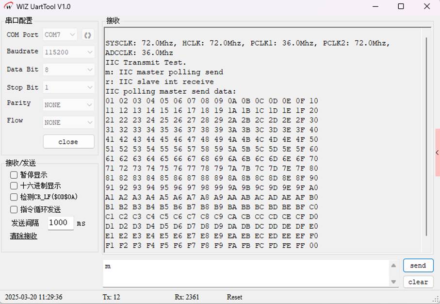
Enter an infinite loop and wait for the user to input a command: input 'm' to execute the I2C master device polling transmission test.
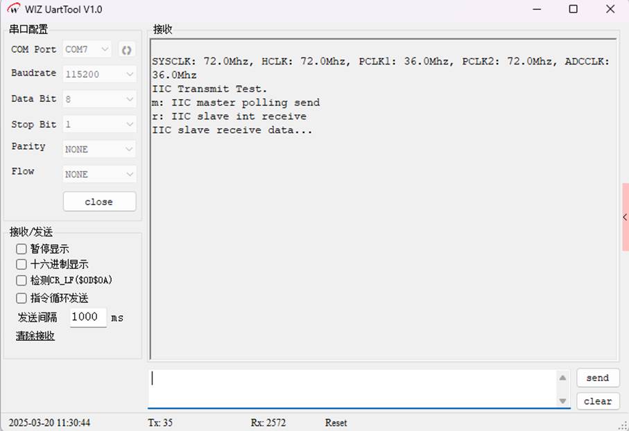
Input 'r' to configure the NVIC and execute the I2C slave device interrupt reception test.
5. I2C configuration function IIC_Configuration()
void IIC_Configuration(void)Enable the clocks for GPIOB and I2C1, I2C2.
Configure pins 6 and 7 of GPIOB as re-multiplexed open-drain outputs, and enable internal pull-up.
Initialize I2C1, set the working mode, duty cycle, address mode, own address, clock speed and response enable, and finally enable I2C1.
6. I2C Master Device Test Function IIC_MasterTest()
void IIC_MasterTest(void)Call the FillData() function to fill the sending buffer and print the sent data.
Generate the I2C start signal, wait for the master mode selection event.
Send the slave device address, wait for the master sending mode selection event.
Loop through the data in the sending buffer, wait for the byte sending completion event after each transmission.
Generate the I2C stop signal, wait for the stop signal transmission to be completed.
7. I2C Slave Device Test Function IIC_SlaveTest()
void IIC_SlaveTest(void)Call the FillData() function to fill the sending buffer.
Enable the events, buffers and error interrupts of I2C1.
Enter an infinite loop. When the RecvFlag is set to 1, print the received data, compare the received and sent data. If they are the same, output the success message for reception, then clear the receiving buffer and reset the RecvFlag.
8. NVIC configuration function NVIC_Configuration()
void NVIC_Configuration(void)Configure the priorities of the event and error interrupts for I2C1, and enable these two interrupts.
9. There are also some other functions
UART_Configuration(): Configures UART1, setting parameters such as baud rate, data bits, stop bits, etc.
DataPrintf(): Prints the buffer data in hexadecimal format.
FillData(): Fills the sending buffer, with data starting from 0x01 and incrementing by 1.
GetCmd(): Receives the user input command from UART1.
SER_PutChar and fputc(): Redirect the standard output functions, sending characters to UART1.
4.3 Download Verification
Open the serial port debugging assistant on the computer, and download the compiled program to the development board. In the serial port debugging assistant, you can see the debugging information for the EEPROM test:
WIZnet is a fabless semiconductor company founded in 1998. Its products include the Internet processor iMCU™, which utilizes TOE (TCP/IP Offload Engine) technology and is based on a unique patented fully hardwired TCP/IP. The iMCU™ is designed for embedded Internet devices in various applications.
WIZnet has more than 70 distributors globally and has offices in Hong Kong, South Korea, and the United States, providing technical support and product marketing services.
The regions managed by the Hong Kong office include Australia, India, Turkey, and Asia (excluding South Korea and Japan).