
Chapter 17: W55MH32’s SPI - Read-Write Serial FLASH
Chapter 17: W55MH32’s SPI - Read-Write Serial FLASH
Chapter 17: W55MH32’s SPI - Read-Write Serial FLASH
References for this chapter: "W55MH32 Chinese Reference Manual" - SPI section and "Introduction to SPI Bus Protocol".
1 Introduction to the SPI Protocol
The SPI protocol was proposed by Motorola Corporation as a communication protocol (Serial Peripheral Interface), which is a high-speed full-duplex communication bus. It is widely used in devices such as ADC, LCD and MCUs, especially in scenarios where a high communication rate is required.
Now, we will explain the physical layer and the protocol layer of the SPI protocol separately.
1.1 SPI physical layer
The common connection methods between SPI communication devices are shown in the following figure. Common SPI communication systems:
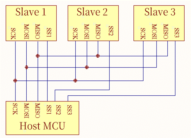
The SPI communication uses three buses and a chip select line. The three buses are SCK, MOSI, and MISO, and the chip select line is SS. Their functions are as follows:
SS (Slave Select): The signal line for selecting the slave device. It is often referred to as the chip select signal line or NSS, and is also called CS. It is represented by NSS. When multiple SPI slave devices are connected to the SPI host, the other signal lines SCK, MOSI, and MISO are simultaneously connected to the same SPI bus, meaning that regardless of the number of slave devices, only these three buses are used; while each slave device has an independent NSS signal line, this signal line exclusively occupies one pin of the host, so there is one NSS signal line for each slave device. In the I2C protocol, devices address and select a certain device on the bus and communicate with it; while in the SPI protocol, there is no device address, it uses the NSS signal line for addressing, when the host wants to select a slave device, it sets the NSS signal line of that slave device to a low level, and that slave device is selected, that is, the chip select is valid, and then the host begins SPI communication with the selected slave device. Therefore, SPI communication uses the low level of the NSS line as the start signal and the high level of the NSS line as the end signal.
SCK (Serial Clock): The clock signal line, used for synchronizing the communication data. It is generated by the communication host and determines the communication rate. Different devices support different maximum clock frequencies. For example, the SPI clock frequency of W55MH32 is the maximum of fpclk/2. When two devices communicate, the communication rate is limited by the slower device.
MOSI (Master Output, Slave Input): The output pin for the master device and the input pin for the slave device. The data of the host is output from this signal line, and the data of the slave device is read from this signal line, that is, the direction of data on this line is from the host to the slave.
MISO (Master Input, Slave Output): The input pin for the master device and the output pin for the slave device. The data of the host is read from this signal line, and the data of the slave device is output from this signal line to the host, that is, the direction of data on this line is from the slave to the host.
1.2 Protocol layer
The SPI protocol defines the initiation and termination signals for communication, data validity, clock synchronization, and other related aspects.
1.2.1 The basic communication process of SPI
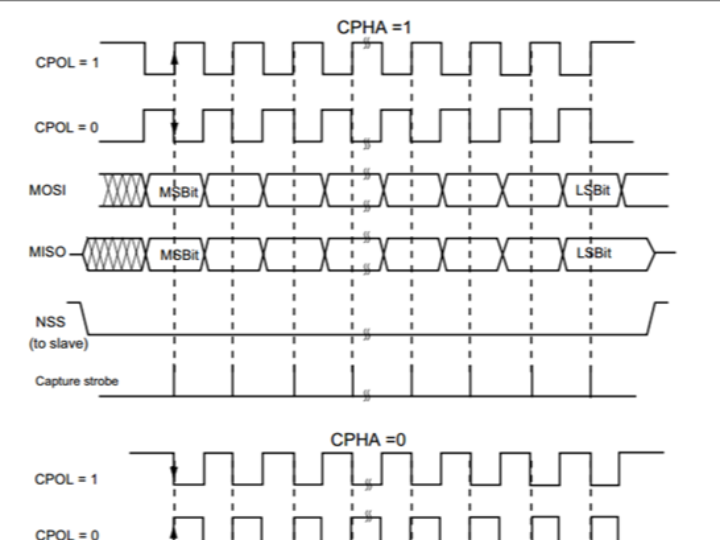
Let's first take a look at the communication timing sequence of SPI communication. See the figure below. SPI communication timing sequence:
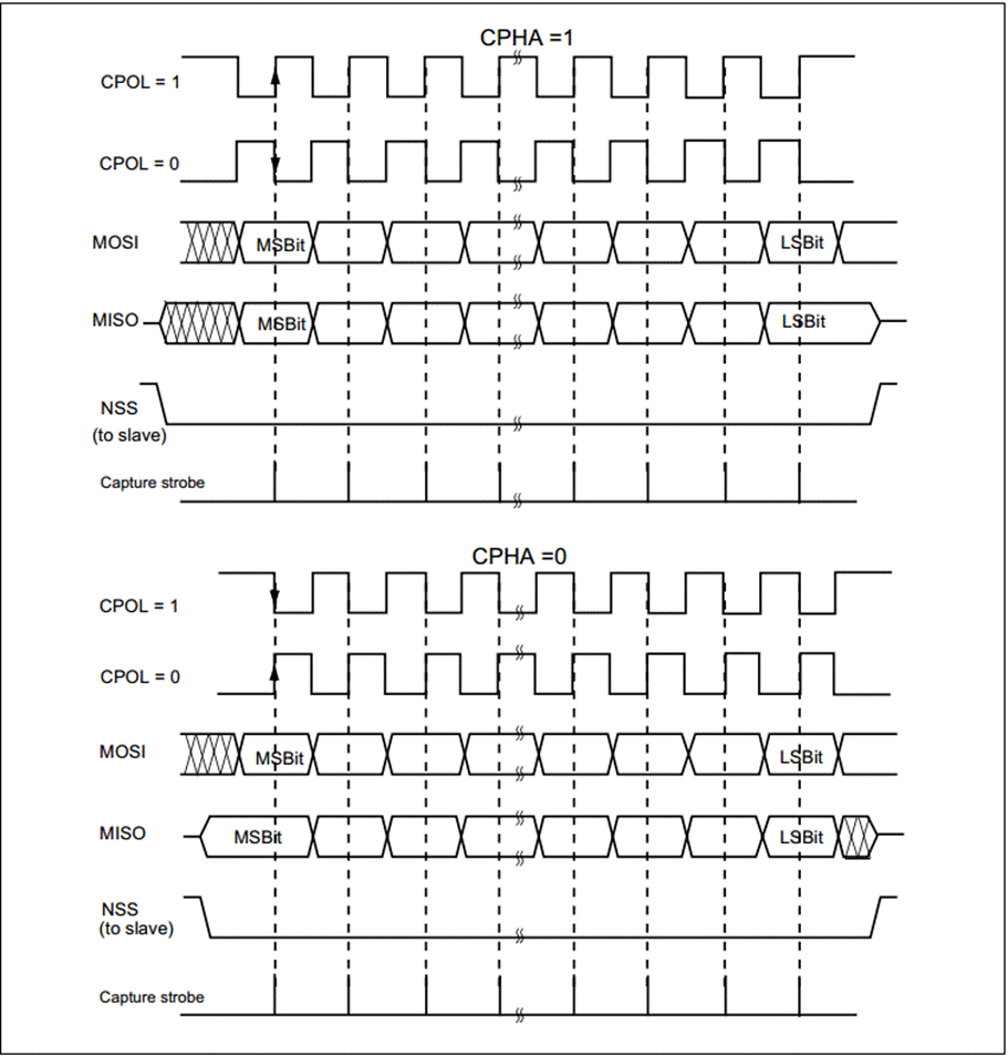
This is the communication timing sequence of the host. The signals NSS, SCK, and MOSI are all generated by the host and controlled by it, while the signal MISO is generated by the slave. The host reads the data from the slave through this signal line. The signals MOSI and MISO are only effective when NSS is at a low level. During each clock cycle of SCK, MOSI and MISO transmit one bit of data.
The decomposition of each signal included in the above communication process is as follows:
1.2.2 The start and stop signals of communication
At the marked positions in the SPI communication timing diagram, the NSS signal line changes from high to low, which is the start signal for SPI communication. NSS is a signal line exclusively occupied by each slave device. When a slave device detects the start signal on its own NSS line, it knows that it has been selected by the host and begins to prepare for communication with the host. At the marked positions in the diagram, the NSS signal changes from low to high, which is the stop signal for SPI communication. It indicates the end of this communication and the selection status of the slave device is cancelled.
1.2.3 Data validity
SPI uses the MOSI and MISO signal lines to transmit data and uses the SCK signal line for data synchronization. The MOSI and MISO data lines transmit one bit of data in each clock cycle of SCK, and data input and output are carried out simultaneously. During data transmission, there is no hard rule regarding whether the most significant bit (MSB) or the least significant bit (LSB) is transmitted first, but it is necessary to ensure that the same protocol is used between the two SPI communication devices. Generally, the MSB-first mode shown in the SPI communication timing diagram is adopted.
By observing the marked areas in the figure, the data of MOSI and MISO changes and outputs during the rising edge of SCK, and is sampled during the falling edge of SCK. That is, at the falling edge of SCK, the data of MOSI and MISO is valid, and when it is at a high level, it represents "1", and when it is at a low level, it represents "0". At other times, the data is invalid, and MOSI and MISO prepare for the next data representation.
SPI can transmit data in units of 8 bits or 16 bits each time, and the number of units transmitted each time is not restricted.
1.2.4 CPOL/CPHA and communication mode
The timing diagram described above in the SPI communication timing is just one of the four communication modes of SPI. SPI has a total of four communication modes. The main differences among them lie in the clock state of SCK when the bus is idle and the data sampling time. To facilitate explanation, the concepts of "clock polarity CPOL" and "clock phase CPHA" are introduced here.
Clock polarity CPOL refers to the level signal of the SCK signal line when the SPI communication device is in an idle state (that is, the state of SCK before the SPI communication starts and when the NSS line is at a high level). When CPOL = 0, SCK is at a low level in the idle state, and when CPOL = 1, it is the opposite.
Clock phase CPHA refers to the sampling time of the data. When CPHA = 0, the signals on the MOSI or MISO data lines will be sampled on the "odd edge" of the SCK clock line. When CPHA = 1, the data lines are sampled on the "even edge" of the SCK.
By different states of CPOL and CPHA, SPI is divided into four modes, as shown in the table below. The four modes of SPI. The host and the slave device need to work in the same mode to communicate normally. In practice, the most commonly used modes are "Mode 0" and "Mode 3":
SPI mode | CPOL | CPHA | Idle time SCK clock | Sampling time |
0 | 0 | 0 | Low voltage | Odd-edge |
1 | 0 | 1 | Low voltage | Even-numbered edges |
2 | 1 | 0 | High level | Odd-edge |
3 | 1 | 1 | High level | Even-numbered edges |
2 The SPI characteristics and architecture of W55MH32
Just like the I2C peripheral, the W55MH32 chip also integrates a peripheral specifically designed for SPI protocol communication.
2.1 Introduction to the SPI peripheral of W55MH32
The SPI interface can be configured to support the SPI protocol or the I2S audio protocol. The SPI interface defaults to working in SPI mode, and the function can be switched from SPI mode to I2S mode through software.
The Serial Peripheral Interface (SPI) enables chips to communicate with external devices in half/full-duplex, synchronous, and serial mode. This interface can be configured in master mode and provides a communication clock (SCK) for external slave devices. The interface can also operate in multi-master configuration.
It can be used for various purposes, including two-wire half/full-duplex synchronous transmission using a single bidirectional data line, and reliable communication with CRC verification.
1. 1.3-wire full-duplex synchronous transmission
2. Two-wire half-duplex synchronous transmission with or without a third bidirectional data line
3. Selection of 8 or 16-bit transmission frame format for master or slave operation, supporting multi-master mode
4. 8 master mode baud rate prescaler coefficients (maximum of fPCLK/2)
5. Slave mode frequency (maximum of fPCLK/2)
6. Fast communication in master mode and slave mode
7. NSS management can be performed by software or hardware in master/slave operation mode: dynamic change of master/slave operation mode
8. Programmable clock polarity and phase, programmable data order, MSB first or LSB first
9. Dedicated sending and receiving flags with trigger interrupt
10. SPI bus busy status flag
11. Hardware CRC for reliable communication
2.2 Analysis of the SPI Architecture of W55MH32
The SPI architecture diagram of W55MH32 is as follows:
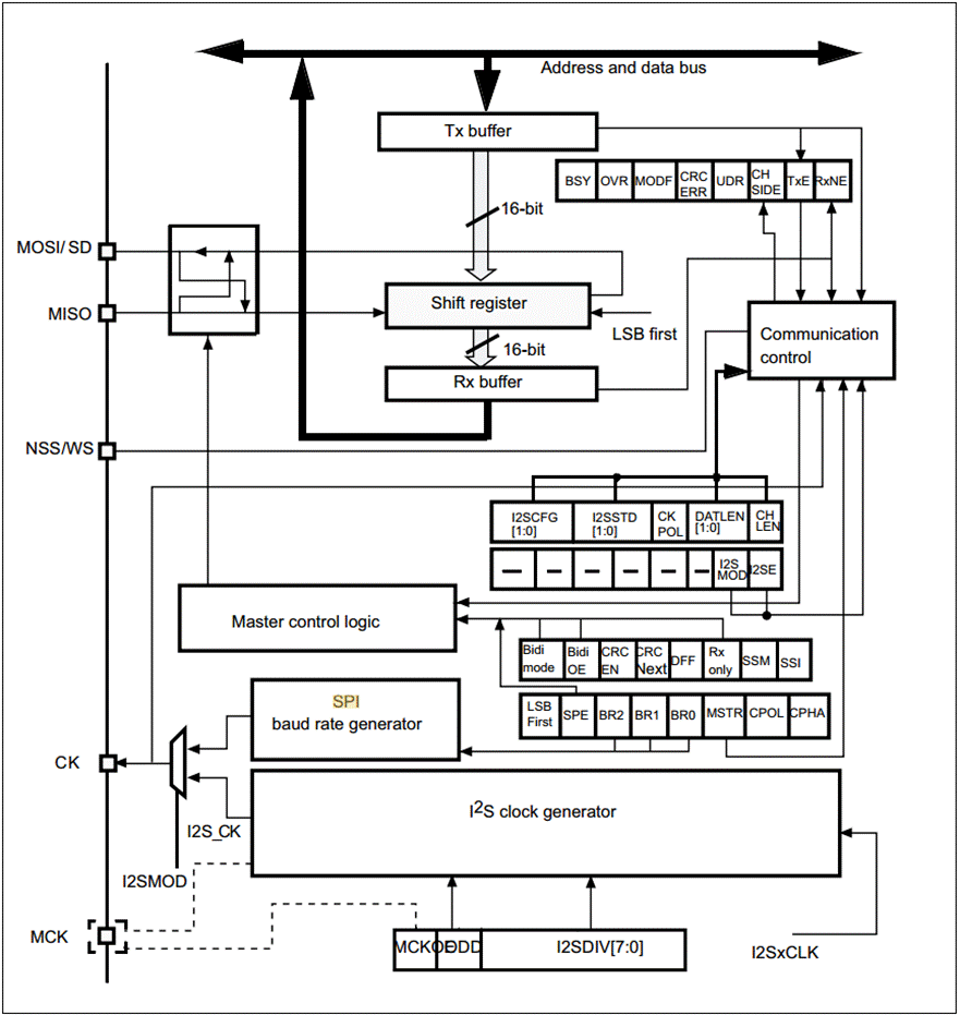
2.2.1 Communication pins
All the hardware architectures of SPI are based on the lines MISO, MOSI, SCK and NSS on the left side of the SPI architecture diagram. The W55MH32 chip has multiple SPI peripherals, and their SPI communication signals are connected to different GPIO pins. When using it, they must be configured to these specified pins as shown in the table below, W55MH32's SPI pins. Regarding the re-mapping function of GPIO pins, please refer to the "W55MH32 Specification", and follow it.
PIN | SPI1 | SPI2 | SPI3 |
NSS | PA4 | PB12 | The TDI of the PA15 download port |
CLK | PA5 | PB13 | TDO of the PB3 download port |
MISO | PA6 | PB14 | NTRST of the PB4 download port |
MOSI | PA7 | PB15 | PB5 |
2.2.4 Overall control logic
The overall control logic is responsible for coordinating the entire SPI peripheral. The working mode of the control logic changes according to the parameters of the "control registers (CR1/CR2)" we have configured. The basic control parameters include the SPI modes, baud rate, LSB first, master-slave mode, single-duplex mode, etc., as mentioned earlier. During the operation of the peripheral, the control logic will modify the "status register (SR)" according to the working status of the peripheral. We can understand the working state of SPI by reading the relevant register bits of the status register. In addition, the control logic is also responsible for controlling the generation of SPI interrupt signals, DMA requests, and controlling the NSS signal line as required.
In practical applications, we generally do not use the standard NSS signal line of the W55MH32 SPI peripheral. Instead, we simply use the ordinary GPIO and control its level output through software, thereby generating the start and stop signals for communication.
2.3 Communication process
In the full-duplex sending and receiving process mode (BIDIMODE = 0 and RXONLY = 0), the software must follow the following process to send and receive data:
1. Set the SPE bit to '1' to enable the SPI module;
2. Write the first data to be sent in the SPI_DR register. This operation will clear the TXE flag;
3. Wait for TXE = 1, then write the second data to be sent. Wait for RXNE = 1, then read the SPI_DR register and obtain the first received data. While reading SPI_DR, the RXNE bit is cleared. Repeat these operations to send the subsequent data while receiving n-1 data;
4. Wait for RXNE = 1, then receive the last data;
5. Wait for TXE = 1, and turn off the SPI module after BSY = 0.
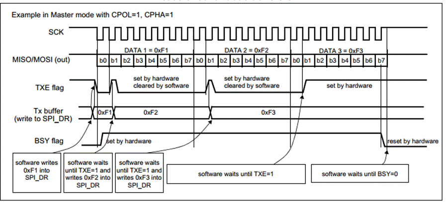
This process can also be implemented in the processing program of the interrupt generated by the rising edge of the RXNE or TXE flag. In the master mode and full-duplex mode (BIDIMODE = 0 and RXONLY = 0) during continuous transmission, the change diagram of TXE/RXNE/BSY is as follows:
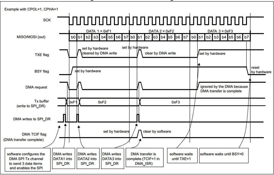
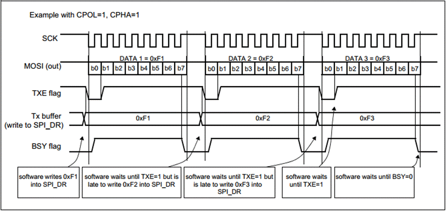
When in continuous transmission mode (BIDIMODE = 0 and RXONLY = 0) in full-duplex mode, the changes in TXE/RXNE/BSY only occur during the transmission process (BIDIMODE = 0 and RXONLY = 0) as shown in the diagram below:
In this mode, the transmission process can be briefly described as follows: wait for the end of transmission by using the BSY bit:
1. Set the SPE bit to "1" to enable the SPI module;
2. Write the first data to be sent into the SPI_DR register. This operation will clear the TXE flag;
3. Wait for TXE = 1, then write the second data to be sent. Repeat this operation to send the subsequent data;
4. After writing the last data into the SPI_DR register, wait for TXE = 1; then wait for BSY = 0, which indicates that the transmission of the last data has been completed. This process can also be implemented in the interrupt handling routine triggered by the rising edge of the TXE flag. Note:
1. For non-continuous transmission, there is a 2 APB clock cycle delay between the operation of writing to the SPI_DR register and the setting of the BSY bit. Therefore, in the single transmission mode, after writing the last data, it is best to wait for TXE = 1 first, and then wait for BSY = 0. 454/671 W55MH32 Reference Manual V1.0.0.
2. In the single transmission mode, after transmitting 2 data, since the received data will not be read, the OVR bit in the SPI_SR register will become '1'. The software does not need to pay attention to this OVR flag.
When performing continuous transmission in the master device's single transmission mode (BIDIMODE = 0 and RXONLY = 0), the diagram of the changes in TXE/BSY is as follows:
When continuous transmission occurs in the device-only transmission mode (BIDIMODE = 0 and RXONLY = 0), the diagram showing the changes in TXE/BSY is as follows:
Bidirectional transmission process (BIDIMODE = 1 and BIDIOE = 1)
In this mode, the operation process is similar to the simple transmission mode. The difference is that before enabling the SPI module, it is necessary to simultaneously set the BIDIMODE and BIDIOE bits in the SPI_CR2 register to "1".
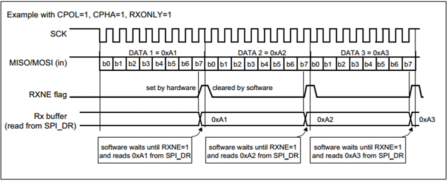
Unidirectional reception-only mode (BIDIMODE = 0 and RXONLY = 1)
In this mode, the transmission process can be briefly described as follows:
1. In the SPI_CR2 register, set RXONLY = 1;
2. Set SPE = 1 to enable the SPI module:
a) In master mode, immediately generate the SCK clock signal and continuously receive serial data before turning off SPI (SPE = 0);
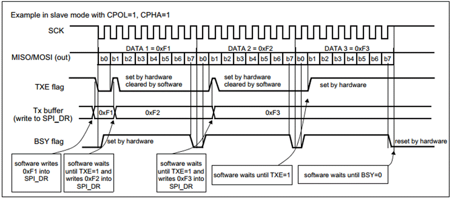
b) In slave mode, when the SPI master device pulls down the NSS signal and generates the SCK clock, receive the serial data.
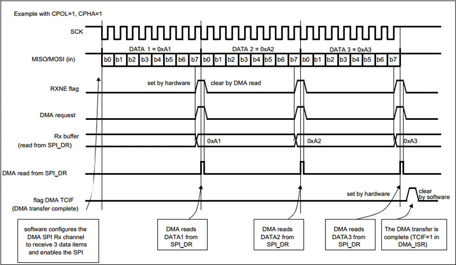
3. Wait for RXNE = 1, then read the SPI_DR register to obtain the received data (and clear the RXNE bit). Repeat this operation to receive all the data.
This process can also be implemented in the interrupt handling routine triggered by the rising edge of the RXNE flag. The diagram of the RXNE change in the continuous transmission mode (BIDIMODE = 0 and RXONLY = 1) is as follows:
Unidirectional reception process (BIDIMODE = 1 and BIDIOE = 0)
In this mode, the operation process is similar to the receive-only mode. The difference is that before enabling the SPI module, it is necessary to set BIDIMODE in the SPI_CR2 register to '1' and clear the BIDIOE bit to '0'.
Continuous and discontinuous transmission
When data is sent in the main mode, if the software is fast enough to detect the rising edge of each TXE (or the TXE interrupt) and immediately write the SPI_DR register before the ongoing transmission ends, continuous communication can be achieved; at this time, the SPI clock remains continuous between each data transmission, and the BSY bit is not cleared.
If the software is not fast enough, it will result in discontinuous communication; at this time, it will be cleared between each data transmission. In the receive-only mode of the main mode (RXONLY = 1), communication is always continuous, and the BSY flag is always '1'.
In the slave mode, the continuity of communication is determined by the SPI master device. Anyway, even if the communication is continuous, the BSY flag will be low for at least one SPI clock cycle between each data item. For non-continuous transmission (BIDIMODE = 0 and RXONLY = 0), the diagram of TXE/BSY changes is as follows:
3 Detailed Explanation of SPI Initialization Structure
Like other peripherals, the W55MH32 standard library provides a SPI initialization structure and initialization function to configure the SPI peripheral. The structure and function definitions are located in the library files "w55mh32_spi.h" and "w55mh32_spi.c". During programming, we can use or refer to the comments in these two files or the library help documentation. After understanding the initialization structure, we can use the SPI peripheral proficiently. See code listing: SPI-1 :
Code Listing: SPI-1 SPI Initialization Structure
1. typedef struct
The descriptions of these structure members are as follows, where the text within the parentheses is the corresponding macro defined for the parameter in the W55MH32 standard library: SPI_DirectionThis member sets the communication direction of the SPI. It can be set to dual-line full-duplex (SPI_Direction_2Lines_FullDuplex), dual-line receiving only (SPI_Direction_2Lines_RxOnly), single-line receiving only (SPI_Direction_1Line_Rx), or single-line transmitting only mode (SPI_Direction_1Line_Tx).
SPI_Mode
This member sets the SPI to operate in either master mode (SPI_Mode_Master) or slave mode (SPI_Mode_Slave). The main difference between these two modes lies in the timing of the SPI SCK signal line. The timing of the SCK signal is generated by the host in the communication. If configured as slave mode, the SPI peripheral of W55MH32 will receive the external SCK signal.
SPI_DataSize
This member can choose whether the data frame size of the SPI communication is 8 bits (SPI_DataSize_8b) or 16 bits (SPI_DataSize_16b).
SPI_CPOL and SPI_CPHA
These two members configure the clock polarity CPOL and clock phase CPHA of SPI. These configurations affect the communication mode of SPI. For the explanations of CPOL and CPHA, please refer to the previous "Communication Mode" section.
The clock polarity CPOL member can be set to high level (SPI_CPOL_High) or low level (SPI_CPOL_Low). The clock phase CPHA can be set to SPI_CPHA_1Edge (collecting data on the odd edge of SCK) or SPI_CPHA_2Edge (collecting data on the even edge of SCK).
SPI_NSS
This member configures the usage mode of the NSS pin. You can choose between the hardware mode (SPI_NSS_Hard) and the software mode (SPI_NSS_Soft). In the hardware mode, the SPI chip select signal is automatically generated by the SPI hardware, while in the software mode, we need to manually pull up or pull down the corresponding GPIO port to generate the non-select and select signals. In practice, the software mode is more commonly used.
SPI_BaudRatePrescaler
This member sets the baud rate divider factor. The divided-down clock becomes the clock frequency of the SPI SCK signal line. This member parameter can be set to a 2x, 4x, 6x, 8x, 16x, 32x, 64x, 128x, 256x division of the fpclk.
SPI_FirstBit
All serial communication protocols have the issue of whether the MSB (most significant bit) comes first (with the high-order data at the front) or the LSB (least significant bit) comes first (with the low-order data at the front). The SPI module of W55MH32 can control this feature through this structure member.
SPI_CRCPolynomial
This is the polynomial used in the CRC check of SPI. When we use CRC check, we use the parameters of this member (the polynomial) to calculate the CRC value.
After configuring these structure members, we need to call the SPI_Init function to write these parameters into the registers to achieve the initialization of SPI, and then call SPI_Cmd to enable the SPI peripheral.
4 SPI—DMA
4.1 Programming essentials
1. Initialize the target pins and port clocks for communication;
2. Enable the clock of the SPI peripheral;
3. Configure the mode, address, rate, etc. parameters of the SPI peripheral and enable the SPI peripheral;
4. Write the basic function for SPI byte transmission and reception;
5. Write the functions for FLASH erasure and read/write operations;
6. Write the test program to verify the read/write data.
4.2 Code analysis
This code implements SPI master mode DMA data transmission for the W55MH32 microcontroller, allowing data to be sent at high speed to the SPI bus through the DMA controller.
1. Overall structure
1. #include "w55mh32.h"
Include the header files related to the chips and the custom delay function.
Define the size of the SPI buffer (256 bytes), and fill the sending buffer with 0x01, 0x02, ..., 0xFF.
2. Main function main
1. int main(void)
Function: Using the SPI master mode and DMA, 256-byte data (SPI_TX_BUFF) is sent at high speed.
Process: Initialization → Fill the buffer → Select signal is valid → Start DMA transmission → Wait for completion → Select signal is invalid.
3. SPI Configuration SPI_Configuration
1. void SPI_Configuration(void)
SPI parameters: Master mode, Full duplex, 8-bit data.
Clock Polarity (CPOL): High level (SPI mode 3).
Clock Phase (CPHA): Sample on the second edge.
Baud Rate: System clock / 256 (low speed, suitable for debugging).
Pin Assignment:
PA4: Chip Select (CS, software controlled).
PA5: SCK (SPI clock).
PA6: MISO (Master Input).
PA7: MOSI (Master Output).
4. DMA Configuration in function DMA_Configuration
1. void DMA_Configuration(void) DMA Channel 3 (Transmit):
● Direction: Memory (SPI_TX_BUFF) → Peripheral (SPI1->DR).
● Trigger Source: SPI1 Send Buffer Empty (TXE flag).
DMA Channel 2 (Receive):
● Direction: Peripheral (SPI1->DR) → Memory (SPI_RX_BUFF).
● Trigger Source: SPI1 Receive Buffer Full (RXNE flag).
Note: In the code, only the transmit channel (DMA1_Channel3) is enabled, and the receive channel is not used.
5. Serial port configuration (used for printing debugging information)
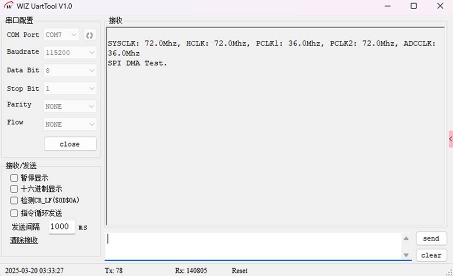
1. void UART_Configuration(uint32_t bound) The serial port is used to print the system clock information (executed only once during initialization).
It has no actual data reception function and is only used for debugging output.
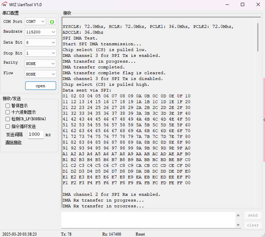
4.3 Download Verification
Open the serial port debugging assistant on the computer, and download the compiled program to the development board. In the serial port debugging assistant, you can see the debugging information of the test:
If you want to know the specific execution steps, you can add the following code during initialization:
1. SPI_Configuration();The following is the debugging information printed during the program execution process:
WIZnet is a fabless semiconductor company founded in 1998. Its products include the Internet processor iMCU™, which utilizes TOE (TCP/IP Offload Engine) technology and is based on a unique patented fully hardwired TCP/IP. The iMCU™ is designed for embedded Internet devices in various applications.
WIZnet has more than 70 distributors globally and has offices in Hong Kong, South Korea, and the United States, providing technical support and product marketing services.
The regions managed by the Hong Kong office include Australia, India, Turkey, and Asia (excluding South Korea and Japan).