
Chapter 16: Introduction of the Common Memory Devices
The introduction of the Common Memory Devices. This is a general information for common memory devices and W55MH32 are related to some of those devices
Chapter 16: Introduction of the Common Memory Devices
1 Types of memory
Memory is an important component of the computer structure. Memory is a part used to store program codes and data. With memory, computers acquire the ability to remember. The basic types of memory are shown in the following figure. Basic types of memory:
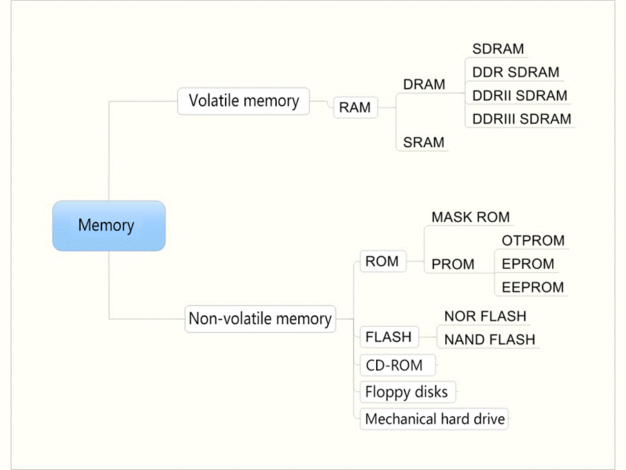
Memory is mainly divided into two categories based on its storage medium characteristics: "volatile memory" and "non-volatile memory". The term "volatile/non-volatile" refers to the property of whether the data stored in the memory will be lost when the power is turned off. Due to the fast access speed of general volatile memory and the ability of non-volatile memory to store data for a long time, they both play important roles in computers. In computers, the most typical representative of volatile memory is the RAM, while the representative of non-volatile memory is the hard disk.
2 RAM memory
RAM is the abbreviation of "Random Access Memory", which is translated as random memory. The term "random access" means that the time required to read or write information in the memory is independent of the position of that information. The origin of this term is because early computers used magnetic drums as memory devices. Magnetic drums are sequential read-write devices, while RAM can read data from any internal address, and the time is the same. Hence, it got its name. In fact, nowadays RAM is specifically used to refer to the volatile semiconductor memory used as computer memory. According to the storage mechanism of RAM, it is divided into two types: Dynamic Random Access Memory (DRAM) and Static Random Access Memory (SRAM).
2.1 DRAM
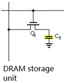
The storage units of dynamic random access memory (DRAM) represent data by the charge of capacitors. A charged capacitor represents 1, and an uncharged capacitor represents 0. See the diagram below, DRAM storage unit. However, over time, the capacitor representing 1 will discharge, and the capacitor representing 0 will absorb charge. Therefore, it needs to undergo regular refresh operations, which is the characteristic described by the term "dynamic". The refresh operation checks the capacitor. If the charge is greater than half of the full charge, it is considered to represent 1 and the capacitor is fully charged; if the charge is less than 1/2, it is considered to represent 0 and the capacitor is discharged to ensure the correctness of the data.
2.1.1 SDRAM
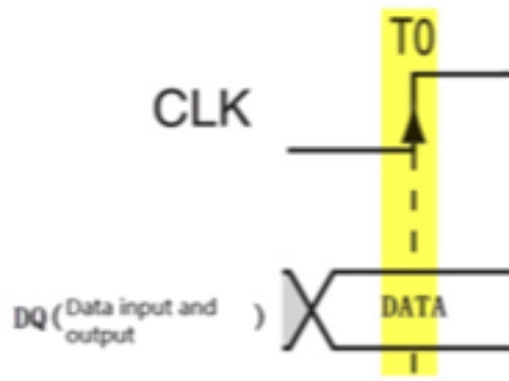
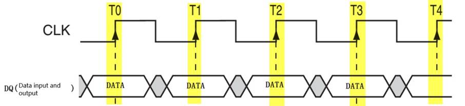
According to the communication mode of DRAM, it can be divided into synchronous and asynchronous types. These two types are distinguished based on whether a clock signal is used during communication. The synchronous communication timing diagram shown in the figure is a communication timing diagram that synchronizes using a clock. It indicates valid data at the rising edge of the clock:
Because the communication speed of clock-synchronized technology is faster, synchronous DRAM is more widely used. This type of DRAM is called SDRAM (Synchronous DRAM).
2.1.2 DDR SDRAM
In order to further enhance the communication speed of SDRAM, DDR SDRAM memory (Double Data Rate SDRAM) was designed. Its storage characteristics are the same as those of SDRAM, but SDRAM only indicates valid data on the rising edge of the clock, and can only represent one piece of data within one clock cycle; while DDR SDRAM indicates one piece of data on both the rising and falling edges of the clock, meaning that it can represent two bits of data within one clock cycle. In this way, the speed is doubled compared to the same clock frequency of SDRAM. As for DDRII and DDRIII, their communication methods are not different; the main difference lies in the increased frequency of the communication synchronization clock.
The commonly used memory sticks in current personal computers are DDR III SDRAM memory, and one memory stick contains multiple DDR III SDRAM chips.
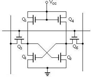
2.2 SRAM
The storage unit of Static Random Access Memory (SRAM) stores data using latches. As shown in the figure below, the SRAM storage unit. This circuit structure does not require periodic refreshing and charging to maintain the state (of course, if the power is cut off, the data will still be lost), so this type of memory is called "static (Static)" RAM.
Similarly, SRAM is classified into synchronous (SSRAM) and asynchronous SRAM based on its communication method. Generally speaking, asynchronous SRAM is more widely used.
2.3 The application scenarios of DRAM and SRAM
By comparing the structures of DRAM and SRAM, it can be seen that the structure of DRAM is much simpler. Therefore, to produce the same capacity of memory, the cost of DRAM is lower and its integration level is higher. However, the capacitor structure in DRAM determines that its access speed is not as fast as that of SRAM. The feature comparison is shown in the following table. Comparison between DRAM and SRAM:
Characteristics | DRAM | SRAM |
Access speed | Slower | Faster |
Integration level | Higher | Lower |
Production cost | Lower | Higher |
Do you need to refresh | YES | NO |
Therefore, in practical applications, SRAM is mainly used as the high-speed cache (Cache) within the CPU, while the external expanded memory typically uses DRAM.
3 Non-volatile memory
There are numerous types of non-volatile memory. Among them, semiconductor-based ones include ROM and FLASH. The others include optical discs, floppy disks, and mechanical hard drives.
3.1 ROM memory
ROM is the abbreviation of "Read Only Memory", meaning a memory that can only be read. With the development of technology, later ROMs that allow for easy data writing were designed. The name "Read Only Memory" was thus retained and is now commonly used to refer to non-volatile semiconductor memory, including the FLASH memory to be introduced later. Some people also classify it within the ROM category.
3.1.1 MASK ROM
MASK (Mask) ROM is the genuine "Read Only Memory". The data stored within it is solidified using special processes during the manufacturing process and cannot be modified after production. Its main advantage is that it has low production costs for large-scale production. Currently, it is still applied in scenarios where there is a large production volume and the data does not need to be modified.
3.1.2 OTPROM
OTPROM (One Time Programmable ROM) is a type of programmable memory. When this memory is manufactured, it does not contain any data internally. Users can use a dedicated programmer to write their own data into it, but this can only be done once. Once written, its content cannot be modified anymore. In the controller chips produced by NXP, OTPROM is often used to store keys or unique MAC addresses of devices, among other things.
3.1.3 EPROM
EPROM (Erasable Programmable ROM) is a type of rewritable memory. It solves the problem that PROM chips can only be written to once. This memory uses ultraviolet light to erase data inside the chip. Both erasing and writing require special equipment. Currently, this type of memory has largely been phased out and has been replaced by EEPROM.
3.1.4 EEPROM
EEPROM (Electrically Erasable Programmable ROM) is an electrically erasable memory. EEPROM can be repeatedly erased. Both its erasure and writing processes are directly controlled by circuits and do not require the use of external devices for erasing. Moreover, data can be modified in units of bytes without erasing the entire chip. Currently, the ROM chips mainly used are all EEPROMs.
3.2 FLASH memory
Flash memory is also known as flash storage. It is a rewritable memory. Some books refer to Flash memory as FLASH ROM, but its capacity is generally much larger than EEPROM. During erasure, it usually erases in units of multiple bytes. For example, some Flash memory has a sector size of 4096 bytes, and the minimum erasure unit is one sector. Depending on the different circuitry of the storage unit, Flash memory is divided into NOR FLASH and NAND FLASH. See the table below for a comparison of the characteristics of NOR_FLASH and NAND_FLASH:
Characteristics | NOR FLASH | NAND FLASH |
Cost of storage with the same capacity | More expensive | Cheaper |
Integration level | Lower | Higher |
Medium type | Random storage | Continuous storage |
Address lines and data lines | Separate independently | Shared |
Eraser unit | Erasure by "sector / block" | Erasure by "sector / block" |
Reading and Writing Unit | Can be based on byte reading and writing | It must be read and written in "blocks" units. |
Reading speed | Higher | Lower |
Writing speed | Lower | Higher |
Bad block | Less | A lot of |
Do you support XIP | Support | Not supported |
The common feature of NOR and NAND is that both require an erasure operation before data writing, and the erasure operation is generally carried out in units of "sectors/blocks". The difference in characteristics between NOR and NAND mainly results from whether the internal "address/data lines" are separated.
Since the address lines and data lines of NOR are separated, it can read and write data in "bytes", which meets the requirements of CPU instruction decoding and execution. Therefore, if the code is stored on NOR, the CPU can give it an address, and NOR can return a data to the CPU for execution without any additional processing operations.
However, since the data and address lines of NAND share, data can only be read and written in "blocks". If the code is stored on NAND, the CPU cannot directly return the data at that address, so it does not meet the requirements of instruction decoding. The last item in the comparison of NOR_FLASH and NAND_FLASH characteristics, "whether it supports XIP", describes this immediate execution feature (Execute In Place).
If the code is stored on NAND, it can be first loaded into the RAM memory, and then executed by the CPU. Functionally, NOR can be regarded as a type of RAM that does not lose data after power loss, but its erasure unit is different from that of RAM, and its read/write speed is much slower than RAM.
In addition, the erasure times of FLASH are limited (currently around 100,000 times). When its usage approaches the lifespan, write operations may fail. Since NAND is usually erased in whole blocks, a single bit failure within a block will cause the entire block to fail, which is called a bad block. Moreover, due to the complex erasing process, NOR blocks are generally fewer and have a longer lifespan than RAM. Due to the possibility of bad blocks, FLASH memory requires "probing/error correction (EDC/ECC)" algorithms to ensure the correctness of the data.
Due to the differences in the characteristics of the two FLASH storage types, NOR FLASH is generally used in scenarios where code is stored, such as the program storage space inside embedded controllers. While NAND FLASH is generally used in scenarios where large amounts of data are stored, including SD cards, USB drives, and solid-state drives, they are all of the NAND FLASH type.
WIZnet is a fabless semiconductor company founded in 1998. Its products include the Internet processor iMCU™, which utilizes TOE (TCP/IP Offload Engine) technology and is based on a unique patented fully hardwired TCP/IP. The iMCU™ is designed for embedded Internet devices in various applications.
WIZnet has more than 70 distributors globally and has offices in Hong Kong, South Korea, and the United States, providing technical support and product marketing services.
The regions managed by the Hong Kong office include Australia, India, Turkey, and Asia (excluding South Korea and Japan).