
Chapter 14: W55MH32’s USART - Serial Communication
Chapter 14: W55MH32’s USART - Serial Communication
Chapter 14: W55MH32’s USART - Serial Communication
References for this chapter: "W55MH32 - Reference Manual" - USART section.
When studying this chapter, it is recommended to read it in conjunction with the USART section of "W55MH32 - Reference Manual". The effect will be better, especially for the parts related to register explanations. Special note: The content of this book is based on the resource explanations of the W55MH32 series controller.
1 Introduction to Serial Communication Protocol
Serial communication (Serial Communication) is a very common serial communication method between devices. Because it is simple and convenient, most electronic devices support this communication method. Electronic engineers also frequently use this communication method to output debugging information when debugging devices.
In computer science, most complex problems can be simplified through layering. For example, chips are divided into the core layer and on-chip peripherals; the W55MH32 standard library is a software layer between registers and user code. For communication protocols, we also understand them in a layered manner. The most basic division is to divide it into the physical layer and the protocol layer. The physical layer specifies the characteristics of the mechanical and electronic components in the communication system, ensuring the transmission of raw data over physical media. The protocol layer mainly defines the communication logic, unifying the data packaging and unpacking standards for both sending and receiving parties. In simple terms, the physical layer determines whether we communicate with our mouths or our bodies, while the protocol layer determines whether we communicate in Chinese or English.
Now, let's explain the physical layer and protocol layer of the serial communication protocol separately.
1.1 Physical layer
The physical layer of serial communication has many standards and variations. We will mainly discuss the RS-232 standard. The RS-232 standard mainly stipulates the usage of signals, communication interfaces, and the electrical level standards of signals.
The common communication structure between serial port devices using the RS-232 standard is shown in the following figure. Serial port communication structure diagram:

In the above communication method, the "DB9 interfaces" of the two communication devices are connected through a serial signal line, and the data signals are transmitted using the "RS-232 standard" on this serial signal line. Since the signals of the RS-232 level standard cannot be directly recognized by the controller, these signals will be converted into the "TTL standard" level signals that the controller can recognize by passing through a "level conversion chip", so that communication can be achieved.
1.1.1 Level standard
Depending on the different level standards used in communication, serial communication can be divided into TTL standard and RS-232 standard. Please refer to the table below. TTL level standard and RS232 level standard:
Communication standard | Level standard (transmitter side) |
5V TTL | Logic 1:2.4V–5V Logic 0:0~0.5V |
RS-232 | Logic 1:-15V~-3V Logic 0:+3V~+15V |
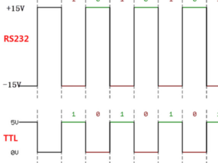
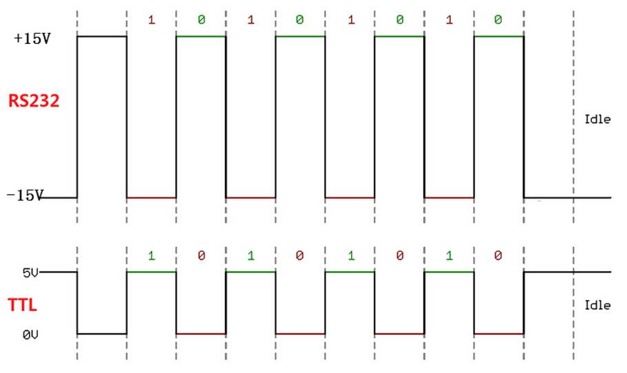
We know that in common electronic circuits, the TTL level standard is often used. Ideally, 5V represents binary logic 1 and 0V represents logic 0. To enhance the long-distance transmission and anti-interference capabilities of serial port communication, -15V is used to represent logic 1 and +15V to represent logic 0. The comparison of RS232 and TTL level calibration when representing the same signal is shown in the following figure. RS-232 and TTL level standards represent the same signal:
Since the controller generally uses the TTL level standard, the MAX3232 chip is often used to convert signals between TTL and RS-232 levels.
1.1.2 RS-232 signal line
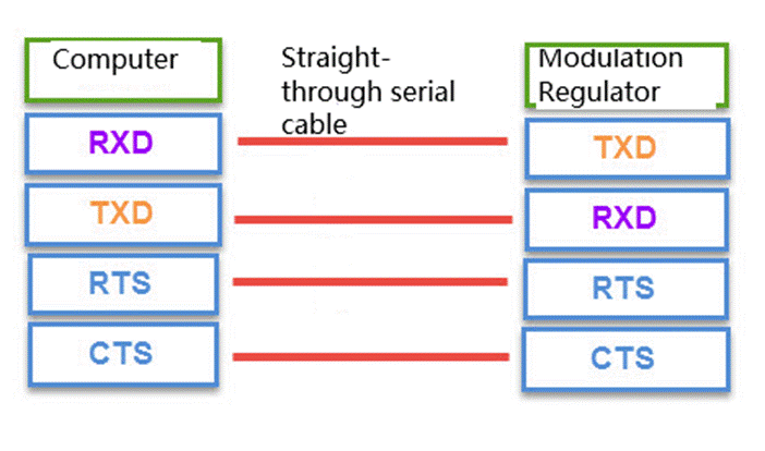
In the initial applications, the RS-232 serial port standard was commonly used for communication between computers, routers and modems (commonly known as "cats"). In this communication system, devices were divided into data terminal equipment DTE (computers, routers) and data communication equipment DCE (modems). We will explain the connection methods of their signal lines and the functions of each signal line based on this communication model.
In traditional desktop computers, there is usually an RS-232 standard COM port (also known as DB9 interface), as shown in the figure below. The COM port and serial port cable on the computer motherboard:
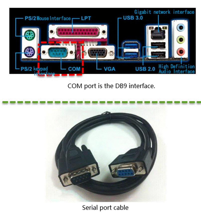
One of the ports to pin out the signal line is known as the male connector, the hole to lead the signal line is known as the female connector. In the computer generally lead to the male interface, and in the modem equipment generally lead to the female connector, the use of the serial cable in the figure above can be connected to the computer. Communication, the serial line in the transmission of the signal is the use of the previously explained RS-232 standard modulation.
In this application, the DB9 interface in the male and female pins of the various pins of the standard signal line connection is shown in the figure below, DB9 standard male and female connection is shown in the table below, DB9 signal line description :
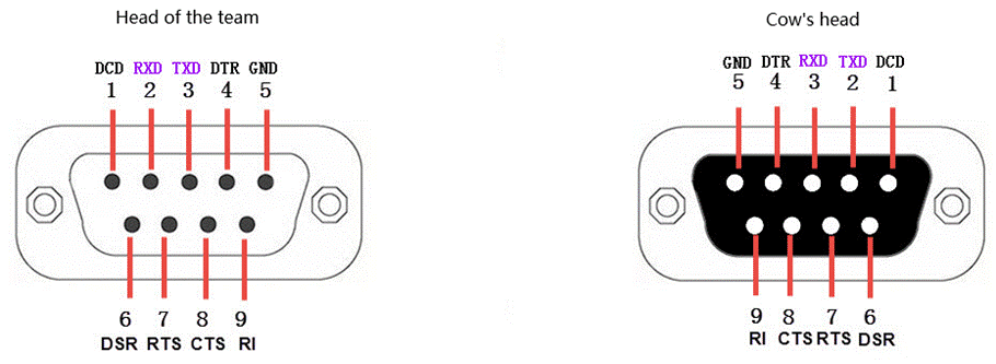
Serial Number | Name | Symbol | Data direction | Explanation |
1 | Carrier detection | DCD | DTE→DCE | Data Carrier Detect, Data Carrier Detection, is used by the DTE to inform the other party whether it has received the carrier signal from the other party. |
2 | Receive data | RXD | DTE←DCE | Receive Data - Data Reception Signal, which is the input. |
3 | Send data | TXD | DTE→DCE | Transmit Data: Data transmission signal, which is the output. The TXD and RXD of the two devices should be connected in a cross manner. |
4 | Data Terminal (DTE) is ready | DTR | DTE→DCE | Data Terminal Ready - This term indicates that the DTE (Data Terminal Equipment) is informing the other party whether the device is ready or not. |
5 | Signal site | GND | - | Ground wire. The ground potential between two communication devices may be different, which will affect the level signals of both the sender and the receiver. Therefore, a ground wire connection must be used between the two serial port devices, that is, common ground. |
6 | Data Communication Equipment (DCE) is ready. | DSR | DTE←DCE | Data Set Ready - This indicates that the data transmission is ready. It is used by DCE to inform the other party whether the current machine is in a standby state. |
7 | Request for transmission | RTS | DTE→DCE | Request To Send, Request to send, DTE Request DCE This device sends data to the DCE end. |
8 | Allow sending | CTS | DTE←DCE | Clear To Send" means "allow sending". The DCE responds to the other party's RTS sending request and informs the other party whether data can be sent. |
9 | Ringing indicator | RI | DTE←DCE | Ring Indicator, ringing indication, indicates that the DCE end has been connected to the line. |
The data in the table represents the standard DB9 male connector connection method for the computer end. Since the transmitting and receiving signals (RXD and TXD) between the two communication devices should be connected in a cross manner, the connection method of the transmitting and receiving signals on the DB9 female connector at the modulation interface is generally opposite to that of the male connector. When connecting the two devices, simply use a "dual-purpose" serial cable to connect them together. See the following figure. The signal lines between the computer and the modulation interface:
The RTS, CTS, DSR, DTR and DCD signals in the serial port cable are represented as "valid" by logic 1 and "invalid" by logic 0. For instance, when the control signal DTR on the computer side is set to logic 1, it is to inform the modem at the remote end that this machine is ready to receive data; while 0 indicates that it is not yet ready.
In the current serial communication used in other industrial control systems, only three signal lines, namely RXD, TXD and GND, are typically employed for transmitting data signals directly. Meanwhile, the RTS, CTS, DSR, DTR and DCD signals have been omitted.
1.2 Protocol layer
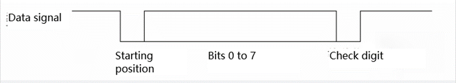
The data packets for serial communication are transmitted from the sending device through its TXD interface to the RXD interface of the receiving device. In the protocol layer of serial communication, the content of the data packets is specified. It consists of the start bit, the main data, the check bit, and the stop bit. For the communication to be able to send and receive data normally, the data packet formats of both parties must be agreed upon. The composition is shown in the following figure. The basic composition of the serial data packet:
1.2.1 Baud rate
This chapter mainly explains the serial interface asynchronous communication, asynchronous communication due to the absence of clock signals (such as the previous explanation of the DB9 interface is not a clock signal), so the two communication devices need to agree on the baud rate, that is, the length of each code element, in order to decode the signal, Figure Serial packets of the basic composition of the dotted line separates each cell is on behalf of a code element. Common baud rates are 4800, 9600, 115200 and so on.
1.2.2 The start and stop signals of the communication
A data packet in serial communication starts with an initial signal and ends with a stop signal. The initial signal of the data packet is represented by a data bit of logic 0, while the stop signal of the data packet can be indicated by 0.5, 1, 1.5 or 2 data bits of logic 1, as long as both parties agree on it.
1.2.3 Valid data
Immediately following the starting bit of the data packet is the main data content to be transmitted, also known as the valid data. The length of the valid data is usually agreed upon to be 5, 6, 7 or 8 bits long.
1.2.4 Data verification
After the valid data comes an optional data check bit. Since data communication is more susceptible to external interference, resulting in deviations in the transmitted data, a check bit can be added during the transmission process to solve this problem. The check methods include odd check, even check, space check, mark check, and no check (noparity).
Odd check requires that the number of "1"s in the valid data and the check bit be odd. For example, an 8-bit valid data is: 01101001. There are 4 "1"s in total. To achieve the effect of odd check, the check bit is "1", and the final transmitted data will be 8 bits of valid data plus 1 bit of check bit, totaling 9 bits.
Even check is the opposite of odd check. It requires that the number of "1"s in the frame data and the check bit be even. For example, the data frame: 11001010. The number of "1"s in the data frame is 4, so the even check bit is "0".
0 check is that regardless of the content of the valid data, the check bit is always "0", while 1 check is that the check bit is always "1".
2 Introduction to USART of W55MH32
The Universal Synchronous Asynchronous Receiver and Transmitter (USART) is a serial communication device that can flexibly exchange full-duplex data with external devices. Different from USART, there is also UART (Universal Asynchronous Receiver and Transmitter), which is a trimmed version of USART that lacks synchronous communication functionality and only supports asynchronous communication. The simple way to distinguish synchronous and asynchronous communication is to see if a clock output is provided externally during the communication. The serial communication we commonly use is basically UART.
Serial communication generally transmits data in frame format, that is, frame by frame transmission. Each frame contains a start signal, data information, stop information, and possibly a check code. USART has specific regulations for these transmission parameters. Of course, there is not only one parameter value, many parameter values can be customized and set. It merely enhances its compatibility.
USART meets the requirements of external devices for the industrial standard NRZ asynchronous serial data format and uses a fractional baud rate generator, which can provide multiple baud rates, making its application more widespread. USART supports synchronous unidirectional communication and half-duplex single-line communication; it also supports local area interconnection networks LIN, SmartCard protocol, and IRDA (Infrared Data Association) SIR ENDEC specifications.
USART supports the use of DMA, enabling high-speed data communication. The specific application of DMA will be explained in the DMA chapter.
USART is most commonly used in the "printing" of program information in the W55MH32 application. Generally, in hardware design, a USART communication interface is reserved to connect to a computer, which can be used to "print" some debugging information on the serial port debugging assistant tool on the computer when debugging the program, so as to understand whether the program is running correctly, where the error occurs, and so on.
3 USART functional block diagram
The functional block diagram of USART includes the core content of USART. Mastering the functional block diagram enables one to have a comprehensive understanding of USART, and when programming, the thinking process will be very clear. The USART functional block diagram is shown in the following figure. USART functional block diagram:
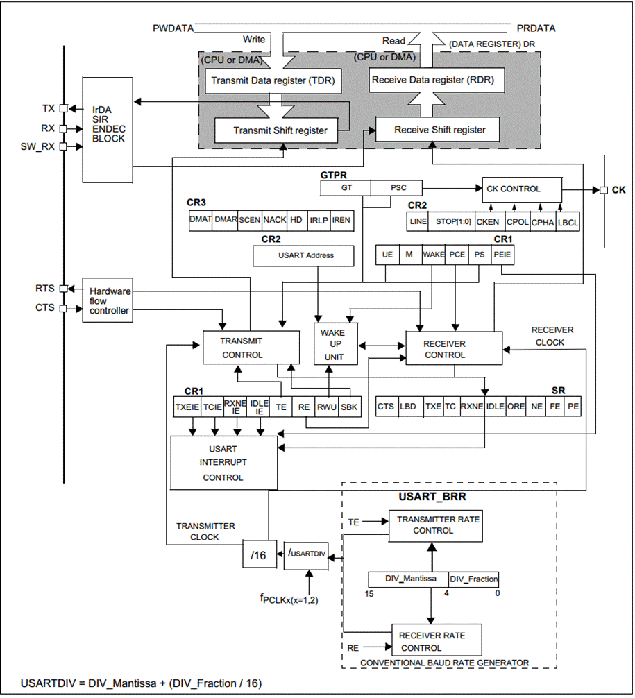
TX: Data output sending pin.
RX: Data input receiving pin.
SW_RX: Data receiving pin, only used in single-line and smart card modes, it is an internal pin and has no specific external pin.
nRTS: Request to send (Request To Send), n indicates low level as valid. If RTS flow control is enabled, when the USART receiver is ready to receive new data, nRTS will be set to low level; when the receive register is full, nRTS will be set to high level. This pin is only applicable to hardware flow control.
nCTS: Clear to send (Clear To Send), n indicates low level as valid. If CTS flow control is enabled, the transmitter will detect the nCTS pin before sending the next frame of data. If it is low level, it indicates that data can be sent; if it is high level, it stops sending after sending the current data frame. This pin is only applicable to hardware flow control.
SCLK: Clock output pin for the transmitter. This pin is only applicable to synchronous mode.
The specific distribution of USART pins on the W55MH32 chip is shown in the following table. The USART pins of the W55MH32 chip:
Pin | APB2 bus (USART1) | APB1 Bus |
|
|
|
| USART1 | USART2 | USART3 | UART4 | UART5 |
TX | PA9 | PA2 | PB10 | PC10 | PC12 |
RX | PA10 | PA3 | PB11 | PC11 | PD2 |
SCLK | PA8 | PA4 | PB12 |
|
|
nCTS | PA11 | PA0 | PB13 |
|
|
nRTS | PA12 | PA1 | PB14 |
|
|
The W55MH32 system controller has three USARTs and two UARTs. Among them, USART1 and the clock source are derived from the APB2 bus clock, with a maximum frequency of 216 MHz. The other four have their clock sources derived from the APB1 bus clock, with a maximum frequency of 108 MHz. UART only has the function of asynchronous transmission, so it does not have SCLK, nCTS, and nRTS function pins.
Data register
The USART data register (USART_DR) is only valid for the lower 9 bits, and whether the 9th bit data is valid depends on the setting of the M bit in the USART control register 1 (USART_CR1). When the M bit is 0, it indicates an 8-bit data word length; when the M bit is 1, it indicates a 9-bit data word length. We generally use an 8-bit data word length.
USART_DR contains the transmitted data or received data. USART_DR actually consists of two registers, one specifically for sending and is writable as TDR, and one specifically for receiving and is readable as RDR. When performing a sending operation, writing data to USART_DR will automatically be stored in TDR; when performing a reading operation, reading data from USART_DR will automatically extract RDR data.
Both TDR and RDR are located between the system bus and the shift register. Serial communication is transmitted bit by bit. When sending, the content of TDR is transferred to the sending shift register, and then the data of the shift register is sent out bit by bit. When receiving, each bit received is sequentially saved in the receiving shift register and then transferred to RDR.
USART supports DMA transmission, which can achieve high-speed data transmission. The specific use of DMA will be explained in the DMA section.
Controller
USART has a transmitter for controlling the transmission, a receiver for controlling the reception, a wake-up unit, interrupt control, and so on. Before using USART, it is necessary to enable USART by setting the UE bit in the USART_CR1 register to 1. The UE bit is used to enable the clock supplied to the serial port.
The data word length for transmission or reception can be selected as 8 bits or 9 bits, controlled by the M bit in USART_CR1.
Transmitter
When the transmit enable bit TE in the USART_CR1 register is set to 1, data transmission is initiated. The data in the shift register will be output at the TX pin, with the lower bits first and the higher bits later. If the synchronous mode SCLK is also output, it will provide the clock signal.
A character frame transmission requires three parts: start bit + data frame + stop bit. The start bit is a low level for one bit period, and the bit period is the time occupied by each bit; the data frame is the 8-bit or 9-bit data we want to send, and the data is transmitted from the lowest bit; the stop bit is a high level for a certain time period.
The length of the stop bit can be controlled by the STOP[1:0] bits in the USART control register 2 (USART_CR2), with options of 0.5, 1, 1.5, and 2 stop bits. The default is 1 stop bit. 2 stop bits are suitable for normal USART mode, single-line mode, and modem mode. 0.5 and 1.5 stop bits are used in smart card mode.
When using 8-bit word length and 1 stop bit, the specific character transmission timing diagram is shown below, and the character transmission timing diagram is:
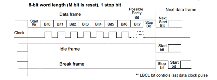
After setting the enable bit TE to 1, the transmitter will first send an idle frame (a high-level frame of the same length as a data frame), and then it can write the data to be transmitted into the USART_DR register. After writing the last data, it is necessary to wait until the TC bit in the USART status register (USART_SR) is 1, indicating that the data transmission is complete. If the TCIE bit in the USART_CR1 register is set to 1, an interrupt will be generated.
When sending data, there are several important flags that we need to summarize when programming:
Name | Description |
TE | Enable transmission |
TXE | The sending register is empty. Use this when sending a single byte. |
TC | The sending is completed. When sending multiple bytes of data, use this method. |
TXIE | Send completion interrupt enable |
Receiver
If the RE bit in the USART_CR1 register is set to 1, the USART receiver is enabled, allowing the receiver to start searching for the start bit on the RX line. Once the start bit is determined, the data is stored in the receiving shift register based on the voltage level on the RX line. After the reception is completed, the data in the receiving shift register is moved to the RDR, and the RXNE bit in the USART_SR register is set to 1. Additionally, if the RXNEIE bit in the USART_CR2 register is set to 1, an interrupt can be generated.
When receiving data, there are several important flags that we will summarize:
Name | Description |
RE | Receiving Enable |
RXNE | Read the non-empty data register |
RXNEIE | Receiver completion interrupt enable |
Generation of fractional baud rate
The baud rate refers to the modulation rate of the data signal on the carrier wave. It is expressed by the number of times the carrier wave's modulation state changes within a unit time, with the unit being baud. The bit rate refers to the number of bits transmitted within a unit time, with the unit being bit/s (bps). For USART, the baud rate and bit rate are equal, and these two concepts will not be distinguished in the future. The higher the baud rate, the faster the transmission rate.
The transmitter and receiver of USART use the same baud rate. The calculation formula is as follows:
Here, fPLCK represents the USART clock, and USARTDIV is an unsigned fixed-point number stored in the baud rate register (USART_BRR). The bits of DIV_Mantissa[11:0] define the integer part of USARTDIV, and the bits of DIV_Fraction[3:0] define the fractional part of USARTDIV.
For example: DIV_Mantissa = 24 (0x18), DIV_Fraction = 10 (0x0A). At this time, the value of USART_BRR is 0x18A. Then, the fractional part of USARTDIV is 10/16 = 0.625; the integer part is 24. Therefore, the value of USARTDIV is 24.625.
If the value of USARTDIV is 27.68, then DIV_Fraction = 16 * 0.68 = 10.88. The closest positive integer is 11, so DIV_Fraction[3:0] is 0xB. DIV_Mantissa = integer (27.68) = 27, which is 0x1B.
Common baud rate values include 2400, 9600, 19200, and 115200. Below is an example to explain how to set the register values to obtain the baud rate value.
We know that USART1 uses the APB2 bus clock, with a maximum of 72 MHz. The maximum frequency for other USARTs is 108 MHz. We select USART1 as an example to explain, so fPLCK = 216 MHz. To obtain a baud rate of 115200 bps at this time:
115200=21600000016/16∗USARTDIV
The result is USARTDIV = 117.1875. By calculation, DIV_Fraction = 0.1875 * 16 = 3 = 0x03, and DIV_Mantissa = 117 = 0x75. Therefore, the value that should be set for USART_BRR is 0x753.
3.1 Verification control
The USART of the W55MH32 series controller supports parity checking. When the parity bit is used, the length of the serial port transmission will be 8 bits of data frame plus 1 bit of parity bit, totaling 9 bits. At this time, the M bit in the USART_CR1 register needs to be set to 1, that is, 9 data bits. By setting the PCE bit in the USART_CR1 register to 1, the parity check control can be enabled. The parity check is automatically completed by the hardware. After enabling the parity check control, the automatic addition of the parity bit will occur when sending the data frame, and the automatic verification of the parity bit will occur when receiving the data. If the parity check fails during data reception, the PE bit in the USART_SR register will be set to 1, and a parity check interrupt will be generated. After enabling the parity check control, the format of each character frame will become: start bit + data frame + parity bit + stop bit.
3.2 Interrupt Control
USART has multiple interrupt request events, as shown in the following table. USART interrupt request:
Interrupt event | Event Indicator | Enable control bit |
The data transmission register is empty. | TXE | TXEIE |
CTS Logo | CTS | CTSIE |
Send completed | TC | TCIE |
Be ready to read the received data | RXNE | RXNEIE |
An overflow error has been detected. | ORE | — |
Idle line detected | IDLE | IDLEIE |
Parity check error | PE | PEIE |
Breaker symbol | LBD | LBDIE |
Noise flags, overflow errors and frame errors in multi-buffer communication | NF/ORE/FE | EIE |
4 Detailed Explanation of USART Initialization Structure
The standard library functions create an initialization structure for each peripheral, such as USART_InitTypeDef. The members of the structure are used to set the working parameters of the peripheral, and are called by peripheral initialization configuration functions, such as USART_Init(). These set parameters will set the corresponding registers of the peripheral to achieve the purpose of configuring the working environment of the peripheral.
The combination of initialization structure and initialization library function is the essence of the standard library. Understanding the meaning of each member of the initialization structure basically enables one to master the use of the peripheral. The initialization structure is defined in the W55MH32_usart.h file, and the initialization library function is defined in the W55MH32_usart.c file. During programming, we can use the comments in these two files for reference.
USART Initializing Structures
typedef struct {USART_BaudRate: Baud rate setting. It is usually set to 2400, 9600, 19200, or 115200. The standard library function will calculate the USARTDIV value based on the set value and then set the value of the USART_BRR register.
USART_WordLength: Data frame word length, which can be 8 bits or 9 bits. It sets the value of the M bit in the USART_CR1 register. If the parity control is not enabled, generally 8 data bits are used; if the parity control is enabled, it is usually set to 9 data bits.
USART_StopBits: Stop bit setting, which can be 0.5, 1, 1.5, or 2 stop bits. It sets the value of the STOP[1:0] bits in the USART_CR2 register. Generally, 1 stop bit is selected.
USART_Parity: Parity control selection, which can be USART_Parity_No (no parity), USART_Parity_Even (even parity), or USART_Parity_Odd (odd parity). It sets the values of the PCE and PS bits in the USART_CR1 register.
USART_Mode: USART mode selection, there are USART_Mode_Rx and USART_Mode_Tx. Two modes can be selected using logical OR operation. It sets the RE and TE bits in the USART_CR1 register.
USART_HardwareFlowControl: Hardware flow control selection. It is only effective in hardware flow control mode. It can be enabled for RTS, enabled for CTS, enabled for both RTS and CTS, or not enabled for hardware flow.
When using synchronous mode, the attribute of the pulse output by the SCLK pin needs to be configured. The standard library uses a clock initialization structure USART_ClockInitTypeDef to set it. The content of this structure is only needed to be set in synchronous mode.
USART Clock Initialization Structure
typedef struct {USART_Clock: Enables the clock output on the SCLK pin in synchronous mode. It can be set to disable the clock output (USART_Clock_Disable) or enable the clock output (USART_Clock_Enable). If synchronous mode is used for transmission, the clock is generally required to be enabled. It sets the value of the CLKEN bit in the USART_CR2 register.
USART_CPOL: Sets the clock polarity on the SCLK pin in synchronous mode. It can be set to low level (USART_CPOL_Low) or high level (USART_CPOL_High) when the SCLK pin is idle. It sets the value of the CPOL bit in the USART_CR2 register.
USART_CPHA: Sets the clock phase on the SCLK pin in synchronous mode. It can be set to capture data on the first edge of the clock (USART_CPHA_1Edge) or on the second edge of the clock. It sets the value of the CPHA bit in the USART_CR2 register. USART_CPHA and USART_CPOL can be used together to achieve various clock relationship modes.
USART_LastBit: Selects whether the clock pulse is output on the SCLK pin when the last data bit is transmitted. It can be set to disable the pulse output (USART_LastBit_Disable) or enable the pulse output (USART_LastBit_Enable). It sets the value of the LBCL bit in the USART_CR2 register.
5 USART_Rs485
5.1 Code analysis
USART1 is used as a debugging terminal (for receiving commands and printing results), while USARTx serves as an RS485 interface (for transmitting and receiving data). The commands and data are detected through polling, demonstrating the basic communication process of the RS485 bus. It is suitable for embedded system development that requires RS485 communication and can serve as the prototype foundation for industrial communication devices (such as Modbus slaves). The core logic is clear, and the hardware details are implemented through the custom rs485.h driver, making it easy to port and expand. The program flow is as follows:
1. Basic Configuration and Dependencies
● Header Files: Include standard library, delay driver (delay.h), hardware abstraction layer (W55MH32.h), and custom RS485 driver (rs485.h).
● Macro Definitions: DATA_LEN specifies the communication data length (5 bytes).
● Global Variables: USART_TEST points to USART1 (debug serial port), rs485buf stores RS485 receive and transmit data.
2. Main Function Flow
● Initialization Phase: System initialization
● delay_init(): Initialize delay function.
● UART_Configuration(115200): Configure USART1 (PA9/TX, PA10/RX) as debug serial port with a baud rate of 115200. Print system clock frequency (SYSCLK/HCLK/PCLK1/PCLK2/ADCCLK).
● RS485 Initialization: RS485_Init(9600): Configure RS485 bus (baud rate 9600). The specific implementation (such as GPIO, USART configuration) is encapsulated in rs485.h.
Main loop logic
int main(void)
{
    uint8_t           key;
    uint8_t           rs485buf[5], i;
    RCC_ClocksTypeDef clocks;

    delay_init();
    UART_Configuration(115200);
    RCC_GetClocksFreq(&clocks);

    printf("\n");
    printf("SYSCLK: %3.1fMhz, HCLK: %3.1fMhz, PCLK1: %3.1fMhz, PCLK2: %3.1fMhz, ADCCLK: %3.1fMhz\n",
           (float)clocks.SYSCLK_Frequency / 1000000, (float)clocks.HCLK_Frequency / 1000000,
           (float)clocks.PCLK1_Frequency / 1000000, (float)clocks.PCLK2_Frequency / 1000000, (float)clocks.ADCCLK_Frequency / 1000000);

    printf("USART RS485 Test.\n");

    RS485_Init(9600); //Initialize RS485

    while (1)
    {
        if (GetCmd() == 's')
        {
            for (i = 0; i < DATA_LEN; i++)
            {
                rs485buf[i] = 0x5A + i;
            }
            RS485_Send_Data(rs485buf, DATA_LEN);
            printf("RS485 Send Data Success\n");
        }

        RS485_Receive_Data(rs485buf, &key);
        if (key) //Data received
        {
            printf("RS485 Recv Data Success\n");
            if (key > DATA_LEN) key = DATA_LEN; //The maximum is 5 data.
            for (i = 0; i < DATA_LEN; i++)
            {
                printf("rs485buf[%d] = 0x%x\n", i, rs485buf[i]);
            }
        }
    }
}
Command detection (USART1 input): Poll the USART1 receive buffer using GetCmd() to check if the character 's' has been received. Once 's' is received, generate test data (0x5A~0x5E) and call RS485_Send_Data to send it.
RS485 data transmission:
● Sending: Periodically send preset data (if interrupts are not used, ensure the switching between receiving and transmitting in half-duplex mode).
● Receiving: Call RS485_Receive_Data to poll for received data. Once received, print the data content through USART1.
Debug output: Output status information (such as successful transmission, received data) through redirected printf.
5.2 Experimental phenomenon
After the program initialization is successful, it will print out the frequencies of each clock and the serial port test information. When we send the character "s", W55MH32 will print out the message indicating that the serial port transmission is successful.
6 Additional Explanation
For the W55M32 chip, the functions or electrical characteristic parameters of each pin can be found in the data manual. The functions and characteristics of the pins and peripherals, as well as the usage of corresponding registers, can be found in the reference manual.
For the W55MH32 chip, when determining to use a certain pin for a certain peripheral function according to the data manual, the following can be consulted in the reference manual: how to configure the GPIO of the peripheral. When the various configurations are unknown, the results obtained from the manual should be taken as the standard.
6.1 TIM1/TIM8 pin configuration
TIM1/TIM8 pins | Configuration | GPIO Configuration |
TIM1/8_CHx | Input capture channel x | Floating input |
TIM1/8_CHx | Output comparison channel x | Push-pull re-usable output |
TIM1/8_CHxN | Complementary output channel x | Push-pull re-usable output |
TIM1/8_BKIN | Brake input | Floating input |
TIM1/8_ETR | External trigger clock input | Floating input |
6.2 Configuration of the pins of the general-purpose timer TIM2/3/4/5
TIM2/3/4/5 pins | Configuration | GPIO Configuration |
TIM2/3/4/5_CHx | Input capture channel x | Floating input |
TIM2/3/4/5_CHx | Output comparison channel x | Push-pull re-usable output |
TIM2/3/4/5_ETR | External trigger clock input | Floating input |
6.3 USART pin configuration
USART pin | Configuration | GPIO Configuration |
USARTx_TX | Full-duplex mode | Push-pull re-usable output |
USARTx_TX | Half-duplex synchronous mode | Push-pull re-usable output |
USARTx_RX | Full-duplex mode | Floating input or pull-up input |
USARTx_RX | Half-duplex synchronous mode | Unused, can be used as general I/O |
USARTx_CK | Synchronization mode | Push-pull re-usable output |
USARTx_RTS | Hardware flow control | Push-pull re-usable output |
USARTx_CTS | Hardware flow control | Floating input or pull-up input |
Regarding the use of serial port interrupts, taking Serial Port 1 as an example, it can be seen from the reference manual, library definitions, and startup files that Serial Port 1 uses USART1_IRQn as an interrupt source and USART1_IRQHandler as an interrupt function. The supplementary explanations in the EXIT section have similar meanings. For Serial Port 1 here, if multiple interrupt flags are enabled, they will trigger interrupts in their respective timing processes. Therefore, in the interrupt function, multiple GetITStatus functions are used to check the flags and perform the corresponding process operations for these flags. Refer to the register descriptions in the manual to understand the timing of each flag and how to clear the flags. Some flags can be cleared using the software clearing process described in the manual and do not need to use the ClearFlag function.
The above supplementary summary is also applicable to the subsequent peripheral learning. Pay attention that there are differences in GPIO configuration and peripherals among different series of chips. The key lies in grasping the overall concept and learning to look up the corresponding content in the manuals of different chips.
WIZnet is a fabless semiconductor company founded in 1998. Its products include the Internet processor iMCU™, which utilizes TOE (TCP/IP Offload Engine) technology and is based on a unique patented fully hardwired TCP/IP. The iMCU™ is designed for embedded Internet devices in various applications.
WIZnet has more than 70 distributors globally and has offices in Hong Kong, South Korea, and the United States, providing technical support and product marketing services.
The regions managed by the Hong Kong office include Australia, India, Turkey, and Asia (excluding South Korea and Japan).