
Development of equipment for organizing a secure information exchange channel based on GOST 28147-89
Consider the implementation of the encryption algorithm GOST 28147-89 using the hardware description languages VHDL and Verilog.
WIZnet - WizFi220
x 1
The SK-iMX53-XC6SLX debug board based on the FreeScale iMX 536 processor (ARM Cortex-A 8 up to 800 MHz) with a wide range of peripherals and high-speed interfaces, built-in 3D coprocessors and a floating-point arithmetic module was used as a debugging tool when developing a data exchange device. dot. The board has a built-in real-time clock with a / 2 C interface, built-in CAN and RS-232 transceivers and 74 input-output lines, to which they can be connected as expansion modules manufactured by Starterkit, and modules developed by the user. The FPGA is a Xilinx Spartan-1 XC6SLX25T chip. The supply voltage of the debug board is 5 V (1-2 A).
On fig. 2.9 shows a block diagram of a device for secure data transmission. To protect the data transmission channel, at least two such devices are required, one of which is connected to the transmitter and encrypts the transmitted data, the second device is connected to the receiver and is designed to decrypt the received data. At the same time, these devices are similar and interchangeable.
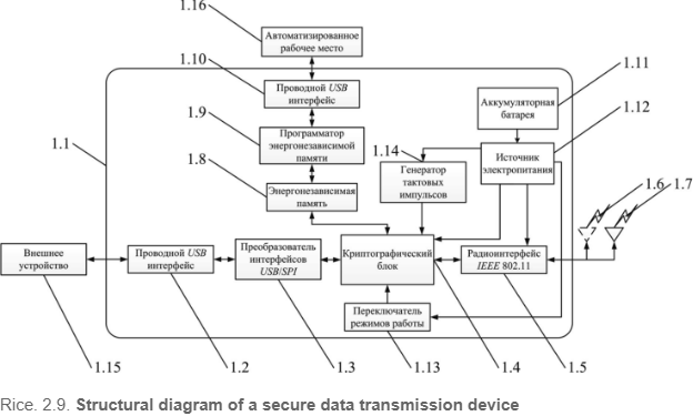
Consider the proposed structure of the device (Fig. 2.9). The device (1.1) includes the following components: wired USB interfaces (1.2, 1.10); interface converter USB/SP1 (1.3); cryptographic block based on FPGA (1.4); radio interface IEEE 802.11 (1.5) with built-in radio antenna (1.7); non-volatile memory (1.8); non-volatile memory programmer (1.9); storage battery (1.11), power supply (1.12); operating mode switch (1.13), clock pulse generator (1.14). It is also possible to connect an external radio antenna (1.6).
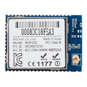
The FT221X chip (FTDI Chip) is used as a USB/SP1 interface converter . Interaction with external devices (1.15) is carried out via a wired USB interface. To ensure interaction with devices via wireless communication channels, the WizFillO module (WIZnet Co.) with a built-in antenna is used, it is also possible to connect an external antenna via the U.FL connector. The WizFi220 module supports IEEE 802.11 blglh wireless standards, WEP and WPA/WPA2 security protocols .Interaction between the module and external devices can be carried out via UART , SPI and I 2 C interfaces.
The key storage device is an electrically erasable reprogrammable read-only memory device 24LC02B (Microchip) with a capacity of 2048 bits, which allows storing eight secret keys of 256 bits each. The interaction between the key storage device and external devices is carried out via the / 2 C interface. The interaction of the non-volatile memory programmer with the automated workplace of an information security specialist (1.16) is carried out via a wired USB interface (1.10). The wideband oscillator DS10S9L (Maxim) is used as a clock pulse generator .
The power supply (1.12) includes five step-down voltage converters and one step-up voltage converter, a MAX 1676 (Maxim) converter is used as a step-up voltage converter, and LM3674 voltage converters (Texas Instruments) are used as step-down voltage converters. Step-down voltage converters are used to provide power
- • FPGA voltage 1.2; 2.5 and 3.3 V;
- • configuration read-only memory required for FPGA operation;
- • radio interface and clock generator.
A boost converter is used to provide power to the non-volatile memory. The interface converter is powered through the power circuits and the common wire of the USB connector.
Two 18650 form factor lithium-ion batteries with a capacity of 3200 mAh are used as rechargeable batteries (1.11), and a 6^24002 charge controller (Texas Instruments) is used to control the process of charging batteries. The process of charging batteries is carried out through the power circuit and the common wire of the USB connector. The charge of two accumulator batteries is enough for 8 hours of continuous work at the maximum possible power consumption.
Consider the structure of the cryptographic block and the purpose of the modules included in its composition (Fig. 2.10).
The cryptographic unit consists of a processor (2.1), a cryptographic coprocessor (2.2), a first SPI transceiver (2.3), a second SPI transceiver (2.4). The cryptographic coprocessor includes a data encryption core (2.5) and a data decryption core (2.6).

Rice. 2.10. Block diagram of a cryptographic block
The main task of the first SPI transceiver is to receive open data packets from external devices and transmit open data packets to external devices, while the direct receiver and transmitter of data is a USB / SPI interface converter , which, in turn, interacts with mobile devices connected via a wired USB interface . Also, the first SPI transceiver provides control over the process of transmitting and receiving data.
The task of the second SPI transceiver is to receive private data packets from external devices and transmit private data packets to external devices, while the direct data receiver and transmitter is the IEEE 802.11 radio interface based on the WizFi220 module , which, in turn, interacts with mobile devices via a wireless communication channel of the standard IEEE 802.11. Also, the second SPI transceiver provides control over the process of transmitting and receiving data.
On fig. Figure 2.11 shows a block diagram of the data encryption kernel, while the structures of the data encryption and decryption kernels are similar. The data encryption and decryption cores are designed respectively to carry out encryption and decryption of binary data sequences in accordance with the encryption algorithm of the GOST 28147-89 standard. The kernels include blocks for performing cryptographic transformations in the modes of simple replacement (4.1), gamma (4.2), and gamma with feedback (4.3). The kernels also include multiplexers (4.5, 4.6) and demultiplexers (4.4, 4.7) designed to switch internal data transmission channels depending on the selected operating mode of the cryptographic coprocessor.

Rice. 2.11. Structural diagram of the data encryption core
In table. 2.7 presents some parameters of the implementation of the GOST 28147-89 cipher algorithm based on FPGA. In this case, the implementation parameters of 32 rounds of data encryption in the simple replacement mode are presented.
The choice of the data encryption/decryption mode is carried out using the operation mode switch. The operating mode switch is a three-contact SHR switcher placed on the surface of the device's printed circuit board. Using the mode switch, the cryptographic coprocessor, which is part of the cryptographic unit, is switched to other modes. The first contact group corresponds to the simple replacement mode, the second - to the gamma mode, the third - to the feedback gamma mode.
Table 2.7
Implementation parameters of the GOST 28147-89 cryptographic transformation algorithm based on FPGA
Family FPGA | Model FPGA | logical cells | Delay, ns | Consumed power | Frequency, MHz | Bandwidth, Mb/s |
Artix-1 | HS7L200 | 3808 | 131,0860 | 0,0730 | 7,6286 | 61,0286 |
Spartan-6 | XC6SLX25 | 3808 | 161,3270 | 0,0290 | 6,1986 | 49,5887 |
The main functions of the processor are:
- • provision of reading information from non-volatile memory, which also includes addressing memory and managing the process of reading information;
- • ensuring interaction with the first and second universal asynchronous UART transceivers , which includes data reception, data transmission, data reception process control, data transmission process control;
- • providing interaction with the cryptographic coprocessor, which includes the transmission and reception of both open and closed data, the control of the processes of receiving and transmitting both open and closed data, the transfer to the cryptographic processor of secret keys previously read from non-volatile memory.
In the process of developing a cryptographic block, a methodology for designing devices based on FPGAs was formulated with the integration of the main design stages into a single cycle. The traditional methodology for designing digital systems based on FPGAs [45] has certain disadvantages, among which it should be noted:
- • the impossibility of an operational assessment of the hardware costs required for the implementation of the designed device;
- • the complexity of modeling when trying to create a mathematical model of the system environment of the designed device, taking into account all possible interference;
- • duration and complexity of the process of converting the mathematical description of the designed device into //DL-description;
- • the need to create an HDL-tqctob to check the created HDL - descriptions, in this case, the problem arises of proving the adequacy of tests on HDL to the tests used at the stage of mathematical modeling.
Based on the listed shortcomings of the traditional design methodology, the task of its modernization becomes relevant. The proposed approach makes it possible to overcome these shortcomings by using data obtained from an FPGA-based device operating in a real circuit in mathematical modeling. The main idea of the proposed design methodology is to integrate the main design stages (mathematical modeling, hardware implementation, debugging as part of the system) into a single iterative design cycle based on the inclusion of additional stages in the design cycle and automation of the process of transferring formalized descriptions of the designed device and data obtained during modeling , as well as system integration between design stages.
The most important point is the automation of the transition from a formal description in the form of a mathematical model to a formal description in the hardware description language. There are a number of tools that allow the transition from a description of a mathematical model in a high-level language to a formal description in a hardware description language, the most famous of which are presented in Table. 2.8.
When working in the MATLAB! Simulink environment , tools such as Xilinx System Generator , Altera DSP Builder , and Simulink HDL Coder are available. The first two tools are designed to work with products of the same companies and work in conjunction with Xilinx ISE and Altera Quartus computer-aided design systems, respectively. The third tool was developed by MathWorks and is included in the MATLAB package . The advantages of the first two include code optimization for specific families of microcircuits and the availability of a number of ready-made components (IP components). Advantage of HDL Coderis universality, since this tool is not tied to specific types of microcircuits or CAD.
Let us consider the main stages of the proposed methodology for designing devices based on FPGAs.
At the first stage, the formalization of the terms of reference for the construction of the system as a whole and the device based on the FPGA in particular and the development of a block diagram, both for the system and for the device, are carried out.
At the second stage, in the MATLAB / Simulink mathematical modeling package , a linearized mathematical model of the system is developed using the floating point format, the developed model is simulated and debugged. During the development of a mathematical model, it seems appropriate to perform the upper level of description at the structural level within the graphical editor of the Simulink package , and to describe individual blocks, use the built-in programming capabilities in M and C languages, as well as use ready-made parameterizable library modules from the Simulink library.Since the linearized model is intended for high-level debugging of the algorithm as part of the simulated system and for evaluating the maximum possible efficiency of the developed algorithm (device, system), the floating point format is usually used to represent data.
An overview of the basic tools that convert a description in a high-level language to a description in a hardware description language
Table 2.8
Name | Developer | Official site | Year development | Input languages | Weekends languages |
Catapult | Calypto | http: //calypto. c om/еп/ pro ducts/catapult/overview | 2004 | C, C++ | RTL |
living Design Suite | Xilinx | http://www.xilinx.com/pr oducts/design- tools/vivado/index.htm | 2012 | С, C++, MATLAB/ Simulink | VHDL, Verilog |
Impulse CoDeve- runner | Impulse Accelerated Technologies | http://www.impulseaccel erated.com/products.htm | 2008 | C, Impulse C | VHDL, Verilog |
High Designer | High | http://www.altium.eom/e п/products/altium- designer | 2008 | S | VHDL, Verilog |
Mitron SDK | Mitronics | http://www.mitrionics.co m/index627f.html?page= developers | 2005 | Mitrion-C | VHDL |
MATLAB HDL Coder | Math Works | http ://www.mathworks.c om/products/hdl-coder/ | 2007 | MATLAB, Simulink, Stateflow | VHDL, Verilog |
C-to- Verilog | Nadav Rotem (. Haifa University) | http://www.c-to- verilog.com/ | 2009 | S | Verilog |
CoolKit | SP6GU | http://oops.math.spbu.ru/ projects/coolkit | 2008 | HaSCol | VHDL |
At the third stage, the algorithm implemented in the floating-point format is converted into a format with the representation of fixed-point numbers and the bit depth is optimized in terms of minimizing hardware costs. To control the correctness of the transformation of the mathematical model, the system is simulated in the same environment, while the system with floating point arithmetic is taken as a reference sample.
At the fourth stage, the blocks of the designed device are replaced with library components oriented for further implementation in the hardware. When using the Altera DSP Builder and Xilinx System Generator packages , it is necessary to replace the building blocks of the Simulink package with similar ones from the hardware development packages. When using the HDL Coder package, no additional steps are required, since this package is based on the standard set of blocks of the Simulink environment. Simulation and comparison with the reference model is also carried out at this stage.
At the fifth stage, hardware-software modeling of the developed device is carried out. To implement the fifth stage, programmable logic computer-aided design systems are used, such as Altera 's Quartus II package or Xilinx 's ISE package and specialized boards with a target FPGA and a set of necessary peripheral tools.
At the sixth stage, debugging and analysis of the parameters of the FPGA-based device in a real system environment are performed. In general, testing requires a programmable arbitrary waveform generator, signal analysis tools such as a spectrum analyzer, logic analyzer, digital oscilloscopes, and FPGA in-circuit debugging tools ( Signal Tap Logic Analyzer - Altera Chip Scope Pro - Xilinx). At the end of the sixth stage, the process of designing an FPGA-based device can be considered completed.
The advantages of the proposed technique for designing devices based on programmable logic integrated circuits are minimizing the influence of the human factor during the transition from a mathematical model of a device to a hardware implementation, the continuity of the device design process, obtaining a debugged mathematical model during the design process, which is a prototype for the device being created and can be used without only during the design process, but also for further optimization of the device operation algorithm based on data obtained from the real system environment of the device being designed.
Debugging and testing of the device for forming a secure information transmission channel was carried out using a debugging complex, which includes a serial development kit
SK-iMX53-XC6SLX and four debug modules, which are the key components of the device (Fig. 2.12). The debug complex includes: USB-SPI interface converter module; IEEE 802.11 radio interface module , which includes a WizFi 220 module with a built-in antenna; a module including a non-volatile memory and a non-volatile memory programmer; a power module that includes a battery and a power supply.

Rice. 2.12. Structural diagram of the debug complex
The USB-SPI interface converter module is designed to provide interaction between the cryptographic unit implemented on the basis of the FPGA and external devices that play the role of sources or receivers of open data. In this case, the module receives an open data message generated by an external device according to the USB standard , the received open message is normalized in accordance with the SPI standard. The FT221X chip ( FTDI Chip manufacturer, SSOP- 28 package) is used as a USB-SPI interface converter chip . A brief technical description of the interface converter is presented in Table. 2.9.
The appearance of the printed circuit board of the USB-SPI interface converter module is shown in fig. 2.13. The module includes the following components: USB connector (1) for connecting external devices; pin connector (2) designed to select the voltage of a high level of the output signal by setting the jumpers to one of two possible positions (position 1-2 - 3.3 V, position 2-3 - 5 V); switch (3) designed to reset the USB-SPI interface converter in case of incorrect operation; FT22XX USB-SPI interface converter chip (4); pin connector (5) for connecting the USB-SPI interface converter moduleto the serial development kit via a flexible cable.
Table 2.9
Brief technical characteristics of the FT221X USB-SPI interface converter
Parameter | Meaning |
Supported USB standard | USB 2.0 |
Transmitter Buffer | 512 bytes |
Receive Buffer | 512 bytes |
Transfer rate | 1 MB/s |
Output high voltage | 2.97...5 V |
Output Low Voltage | 0..D4V |
Supply voltage | 2.97...5.5 V |
Consumption current | 8.1...13.1 mA |
Type of shell | SSOP (20 pins) |
Ambient temperature | -65...150 °C |
Mounting is done on a double-sided printed circuit board. The dimensions of the sides of the printed circuit board are 80x75 mm and comply with GOST R 53429-2009. The thickness of the rigid base is 0.36 mm ( FR4 material), the foil thickness of the upper and lower layers is 35 µm. When performing component placement and PCB routing, the following design rules were adopted:
- • distance between polygon and via - 0.254 mm;
- • distance between landing sites - 0.127 mm;
- • distance between landing pad and via - 0.1 mm;
- • distance between all other elements - 0.127 mm;
- • width of power circuits and common wire routes: minimum - 0.254 mm, recommended - 0.35 mm, maximum - 0.5 mm;
- • width of traces of all other circuits - 0.127 mm;
- • tracing method: either with a predominance of horizontal links, or with a predominance of vertical links (depending on a specific module);
- • diameter of vias: minimum - 0.6 mm, recommended - 0.6 mm, maximum - 0.9 mm;
- • horizontal distance between components - 0.2 mm.

Rice. 2.13. External view of the printed circuit board of the USB-SPI interface converter module
Schematic diagram of the module, placement of elements and PCB tracing are made in the Altium Designer 10 computer-aided design system. The specification of the USB-SPI interface converter module is presented in Table. 2.10.
The IEEE 802.11 radio interface module is designed to provide interaction between an FPGA-based cryptographic unit and external devices that play the role of sources or receivers of private data. The WizFi 220 module (manufactured by WIZnet Co. , Fig. 2.14) with a built-in antenna is used as a radio interface module, it is also possible to connect an external antenna via a U.FL standard connector. Brief technical characteristics of the radio interface module are presented in Table. 2.11.
The radio interface module receives private data messages generated by the second device included in the data transmission protection system or transmits private data messages generated by the cryptographic unit. In this case, the receiver is the second data transmission protection device included in the transmission protection system. Data reception and transmission are carried out in accordance with the IEEE 802.11 (Wi-Fi) standard, interaction with the cryptographic unit is carried out in accordance with the SPI standard.
Table 2.10
USB-SPI Interface Converter Module Specification
Pos. designation | Designation | Quantity |
S1-S2, S4 | Capacitor Epcos XIR - 100nF ±20% | 3 |
NW | Capacitor Epcos 541121 - 4.7uF ±20% | 1 |
DDI | Chip FTDIFT22 X | 1 |
SAI | Switch Conn fly DS 1040 | 1 |
H | USBA-XJ connector | 1 |
XI | Connector PLD- 40, 40 pins, double row | 1 |
xs | Connector PLS- 03, 3 pins, single row | 1 |
RX-R2 | Resistor Vishay D 1 / S50G0603 - 27 Ohm ± 5%, 0.1 W | 2 |
R3 | Resistor Vishay D 1 / S5S1G0603 - 4.7 kOhm ± 5%, 0.1 W | 1 |
R4 | Resistor Vishay DMCRCW0603 - 10 kOhm ±5%, 0.1 W | 1 |
Y | EMI filter Laird MI0805K400R- 10 | 1 |
Table 2.11
Brief technical characteristics of the WizFiHO radio interface module
Parameter | Meaning |
Supported communication protocol | SHEESHMYya/p |
Supported data rates | 1.2, 5.5, 11 Mbps |
Supported network protocols | UDP, TCP/IP (IPv4), DHCP, ARP, DNS, HTTP/HTTPS |
Supported security protocols | WEP, WPA/WPA2-PSK, EAP- FAST, EAP-TLS, EAP-TTLS, PEAP |
Operating frequency | 2.4...2.497 GHz |
I/O interfaces | UART, ~SPI, Yc,WAKE, ALARM, GPIO |
Input high voltage | 2.64...3.3 V |
Low Voltage Inputs | -0.3...0.825 V |
Supply voltage | 3.3V |
Quiescent current consumption | 35...50 μA |
Current consumption in receive mode | 125...130 mA |
Current consumption in transmission mode | 250...260 mA |
Housing dimensions | 32x23.5x3 mm |
Ambient temperature | -40. ..85 °C |
The appearance of the printed circuit board of the IEEE 802.11 radio interface module is shown in fig. 2.14. The module includes the following main components: USB connector (1) for connecting a personal computer when setting up and reprogramming the radio interface module; switch (2) designed to reset the built-in USB-UART interface converter in case of incorrect operation; pin connector (3) for connecting the radio interface module to the power supply module; LEDs (4) designed to control the functioning of the built-in USB-UART interface converter(data transmission, data reception, interface converter power supply); LEDs (5) designed to indicate the operating modes of the WizFi 220 module ( Access Point connection indicator, Serial-to-Wi-Fi status indicator, Serial Data Rx indicator ); built-in interface converter USB-UART FTDI FT232RL (6), designed to ensure the interaction of the radio interface module with a personal computer via the USB interface when configuring and reprogramming the radio interface module; WizFi220 radio interface module(7); tact button (8) designed to wake the radio interface module from sleep mode; tact button (9) designed to reset the radio interface module in case of incorrect operation; tact button (10), designed to bring the settings of the radio interface module to the factory configuration; LED (11) for indicating the power supply status of the WizFi220 radio interface module; pin connector (12) for connecting the IEEE 802.11 radio interface module to a serial development kit via a flexible cable; pin connector (13), designed to switch the operating modes of the WizFi220 radio interface module by setting the jumpers to one of two possible positions (position 1-2 -Run Mode , 2-3 - Program Mode); pin connector (14), designed to switch the operating modes of the WizFi220 radio interface module by setting the jumpers to one of two possible positions (position 1-2 - Data Mode , 2-3 - Command Mode).
The specification of the IEEE 802.11 radio interface module is given in Table. 2.12.
Mounting is done on a double-sided printed circuit board. The dimensions of the sides of the printed circuit board are 75x100 mm and comply with GOST R 53429-2009. The thickness of the rigid base is 0.36 mm ( FR4 materials), the thickness of the foil of the upper and lower layers is 35 µm. Component placement and PCB layout followed the design rules previously defined for the USB-SPI interface converter module board.
Key memory module includes non-volatile memory and non-volatile memory programmer. The 24LC02 electrically erasable reprogrammable read-only memory (EEPROM) chip ( Microchip , SOP- 8 L package ) with a capacity of 2048 bits is used as a key storage device, which allows storing eight secret keys of 256 bits each.

Rice. 2.14. External view of the printed circuit board of the IEEE 802.11 radio interface module
The second EEPROM chip 24LC02 is designed to store the contents of the replacement tables of the GOST 28147-89 cryptographic conversion algorithm. Interaction between the key storage device and external devices is carried out through the / 2 C interface. The interaction of the non-volatile memory programmer with a personal computer is carried out through an interface converter
USB-UART , while the key memory module is connected to a personal computer via a USB interface.
Table 2.12
IEEE 802.11 radio interface module specification
Pos. | Designation | When |
designation | quality | |
VDX-VD1 | Kingbright KA -3022 diode | 7 |
ZQ1 | Quartz resonator Geyer KX-K- 12 MHz | 1 |
S1-S2, S4 | Capacitor EpcosXIR - 100nF ±20% | 3 |
NW | Capacitor Epcos 541121 - 4.7uF ±20% | 1 |
C5-C6 | Capacitor Epcos COG - 27nF ±20% | 2 |
YES 1 | Chip WizNet WizFi 210 | 1 |
DDI | Chip FTDIFT232RL | 1 |
SAX | Switch Connfly DS X 040 | 1 |
SBX-SB3 | TE button FSM4GH | 3 |
XX | Connector PLD- 40, 40 pins, double row | 1 |
XI | Connector PLS- 02, 2 pins, single row | 1 |
HZ-X4 | Connector PLS- 03, 3 pins, single row | 2 |
X5 | USBA-XJ connector | 1 |
R 1-53,55 | Resistor Vishay DX X/CRCW0603 - 4.7 kΩ ±5%, 0.1 W | 4 |
R4 | Resistor Vishay DX X/CRCW0603 - 10 kΩ ±5%, 0.1 W | 1 |
R6-RX2 | Resistor Vishay DX X/CRCW0603 - 270 Ohm ±5%, 0.1W | 7 |
LX | EMI filter Laird М/080554005-10 | 1 |
A brief technical description of the 24LC02 EEPROM chip module is presented in Table. 2.13.
Technical characteristics of EEPROM 24TS02
Table 2.13
Parameter | Meaning |
Capacity | 2 kbit |
Memory organization | 256x8 |
Interface | fc |
Clock frequency | 400 kHz |
Supply voltage | 2.5...5.5 V |
Quiescent current consumption | 5 μA |
Current consumption in read mode | 0.05... 1 mA |
Current consumption in write mode | 0.1 ... 3 mA |
Type of shell | TSSOP (8 pins) |
Ambient temperature | -40... 125 °C |
The appearance of the printed circuit board of the key memory module is shown in fig. 2.15. The module includes the following components: USB connector (1) designed to interact with a personal computer in the process of reprogramming EEPROM chips; pin connector (2) for connecting the key memory module to the power supply module; LEDs (3) designed to control the functioning of the built-in USB-UART interface converter (data transmission, data reception, interface converter power supply); built-in interface converter USB-UART FTDI FT232RL(four); switches (5, 6) designed to transfer the EEPROM chips to the overwrite protection mode; EEPROM chips 24LC02 (7-8); switch (9) designed to reset the built-in USB-UART interface converter in case of incorrect operation; pin connectors (10-11) designed to select the operation mode of the cryptographic unit by setting the jumpers to one of three possible combinations of positions (01 - simple replacement mode, 10 - gamut mode, 11 - gamut mode with feedback); pin connector (12) for connecting the key memory module to the serial development kit via a flexible cable.

Rice. 2.15. External view of the printed circuit board of the key memory module
The specification of the key memory module is presented in Table. 2.14.
Table 2.14
Key Memory Module Specification
Pos. | Designation | When |
designation | quality | |
VDX-VD2 | Diode NXP BZV55 | 2 |
VD3-VD5 | Kingbright KA- 3022 diode | 3 |
ZQI | Quartz resonator GeyerKX-K- 12 MHz | 1 |
S1-S2, S4 | Capacitor Epcos X75 - 100 nF ±20% | 3 |
NW | Capacitor Epcos 541121 - 4.7uF ±20% | 1 |
C5-C6 | Capacitor Epcos COG - 21nF ±20% | 2 |
DDX | Microchip 2ALC02 | 2 |
DD2 | Chip FTDIFT232RL | 1 |
SA1-SA3 | Switch Connfly DS 1040 | 3 |
XI | USBA-IJ connector | 1 |
X2 | Connector PLS- 02, 2 pins, single row | 1 |
xs | Connector PLD- 40, 40 pins, double row | 1 |
X4-X5 | Connector PLS-03, 3 pins, single row | 2 |
51,56,58 | Resistor Vishay DMCRCW0603 - 10 kOhm ±5%, 0.1 W | 3 |
52, 54 | Resistor Vishay DMCRCW0603 - 270 Ohm ±5%, 0.1 W | 2 |
53,55,57 | Resistor Vishay DXICRCW0603 - 4.7 kOhm ±5%, 0.1 W | 3 |
59,510,511 | Resistor Vishay DXICRCW0603 - 270 Ohm ±5%, 0.1 W | 3 |
11 | EMI filter Laird М/0805Х4005-10 | 1 |
Mounting is done on a double-sided printed circuit board. The dimensions of the sides of the printed circuit board are 80x80 mm and comply with GOST R 53429-2009. The requirements and design parameters are the same as for the previously discussed device components.
The power supply module is designed to provide power supply to the key memory modules and the IEEE 802.11 radio interface. The power supply module includes two MAXXY5 DC boost converters (manufacturer Maxim , UMAX 10 package). The first converter is designed to power the key memory module (supply voltage 3.3 V), the second converter is designed to power the IEEE radio interface module802.11 (supply voltage 5 V). The input voltage of the converters comes from rechargeable batteries, which are two lithium-ion batteries of the 18650 form factor and with a capacity of 3200 mAh. The 5024002 controller ( Texas Instruments , R-PDSO-G20 package) is used to control the battery charging process . The process of charging the batteries is carried out through the power circuit and the common wire of the USB connector , so you can charge the batteries from a personal computer or laptop. A brief technical characteristic of the MAX 1676 boost converter is presented in Table. 2.15, charge controller 5024002 - in table. 2.16.
Table 2.15
Brief technical characteristics of the DC boost converter MAX1616
Parameter | Meaning |
Input voltage | 0.7...5.5 V |
Output voltage | 2...5.5 V |
Output current | < 300 мА |
Consumption current | 60 μA |
Quiescent current consumption | 16 μA |
Maximum conversion duty cycle | 94% |
Type of shell | /iMAX( 10 pins) |
Ambient temperature | -40...85 °C |
Table 2.16
Brief technical characteristics of the battery charge controller #? 24002
Parameter | Meaning |
Battery type | Li-Ion |
Input voltage | 4.5...10V |
Output voltage | 4.158...4.242 V |
Supply voltage | 4.5...10V |
Consumption current | 1 mA |
Quiescent current consumption | 1 μA |
Type of shell | TSSOP (20 pins) |
Ambient temperature | -40... 125 °C |
The appearance of the printed circuit board of the power module is shown in fig. 2.16. The module includes: a USB connector (1) designed to charge batteries via USB standard power lines ; battery charge controller BQ 24002 (2); LEDs (3) designed to control the process of functioning of the battery charge controller; LED (4) designed to indicate the low level of battery charge; terminals (5) intended for mounting the Epcos 557M861 thermistor used to control the temperature of the battery shell during the charging process; pin connector (6) for connecting batteries; step-up DC convertersMAXX616 (7-8); pin connector (9) for connecting the power supply module to the power connector of the key memory module via a flexible cable; pin connector (10) for connecting the power supply module to the power connector of the IEEE 802.11 radio interface module using a flexible cable. The specification of the power supply module is presented in table. 2.17.

Rice. 2.16. The appearance of the printed circuit board of the power module
Table 2.17
Power module specification
Pos. designation | Designation | Quantity |
L,L2 | Choke Bourns 5Sh -0805-220MG - 22 µH | 2 |
VD | Diode /L 10M?040N | 1 |
VD2-VD6 | Kingbright KA- 3022 diode | 5 |
VD1 | Diode 77 GS-431 | 1 |
Cl, C4, Cl, C9 | Capacitor Vishay TM - 47 μF ±20 % | 4 |
C2 | Capacitor Cpcos? 41121-10 uF ± 20% | 1 |
C3, C5, C6, C8, CIO | Capacitor Epcos X7R - 100nF ±20% | 5 |
Cll | Capacitor Epcos XIR - 1uF ±20% | 1 |
Cl 2 | Capacitor Epcos XIR - 220nF ±20% | 1 |
DA,DA3 | Chip Maxim MAXX616 | 2 |
DA2 | Chip TIBQ24002 | 1 |
The end of the table. 2.17
Pos. designation | Designation | Quantity |
H1,HZ-H4 | Connector PLS- 02, 2 pins, single row | 3 |
XI | USB connector | 1 |
RI | Resistor Vishay D 1/SDSŽ0603 - OD Ohm ±5 %, OD Wt | 1 |
R2, R8 | Resistor Vishay D 1/SDSŽ)603 - 200 Ohm ±5 %, OD Wt | 2 |
R3,R | Resistor Vishay DMCRCW0603 - 470 kOhm ±5%, OD W | 2 |
R4,RU | Resistor Vishay D 1 / СЯС1Р0603 - 340 kOhm ± 5%, OD W | 2 |
R5,R12 | Resistor Vishay D 1 ICRCm603 - 100 kOhm ±5 %, 0.1 W | 2 |
R6,R4 | Resistor Vishay DICRCW9603 - 270 Ohm ±5%, OD W | 2 |
Rl, R9,R3 | Resistor Vishay DICRCW96№ - 470 Ohm ±5 %, OD Wt | 3 |
R15 | Resistor Vishay D 1 ICRCm603 - 1D kOhm ±5 %, 0.1 W | 1 |
R16 | Resistor Vishay D MCRCW0603 - 1 kOhm ±5%, OD W | 1 |
Rll | Resistor Vishay D 1 / SLSZh0603 - 5.6 kOhm ± 5%, OD W | 1 |
RIS | Resistor Vishay D ICRCW0603 - 18.7 kΩ ± 5%, OD W | 1 |
R19 | Resistor Fw / Shu D11 / SDSZh0603 - 95.3 kOhm ± 5%, OD W | 1 |
RK 1 | Resistor V57M861 - 10 kOhm ± 5%, OD Wt | 1 |

Rice. 2.17. Methodology for designing a device for ensuring secure data transmission
Mounting is done on a double-sided printed circuit board. The dimensions of the sides of the printed circuit board are 100x80 mm and comply with GOST R 53429-2009. The requirements and design parameters are the same as for the previously discussed device components.
The design methodology for the device under consideration can be summarized and presented in the form of an IDEF3 diagram , shown in fig. 2.17. To simulate the device, the environment was used
Simulink, in which the device was represented as a three-channel (three encryption streams) queuing system. The simulation results (Table 2.18) show that the device provides reliable data processing and transmission when using most common wireless interfaces. It is also possible to use the device in conjunction with the USB 3.0 interface when using intermediate drives for incoming data packets.
Table 2.18
The results of modeling a device for the exchange of classified documentary information
Standard | QS operating time, µs | Received applications | Serviced applications | Applications not served |
802.11# | 100 | 56 | 56 | 0 |
802.11l | 100 | 156 | 156 | 0 |
802.1 lac | 100 | 1364 | 1362 | 2 |
Gigabit Ethernet | 100 | 1040 | 1038 | 2 |
Fast Ethernet | 100 | 104 | 104 | 0 |
USB 1.0 | 100 | 12 | 12 | 0 |
USB 2.0 | 100 | 498 | 497 | 1 |
USB 3.0 | 100 | 1915 | 1872 | 43 |
The design methodology and the developed device that provides secure information exchange over industrial wireless data transmission networks can be used in the development of communication tools for integrated information systems that are characterized by the complexity of information exchange processes, while at the same time high requirements for confidentiality of data access. The proposed approach allows solving the problem of organizing secure communication channels using the effective data encryption standard GOST 28147-89, ensuring the protection of wireless data transmission between any devices that support USB and IEEE 802.11 interfaces, which is of particular importance when building integrated information systems for managing energy and industrial facilities. production.