Design Navigation Computer System Based on Double Digital Signal Process and FPGA
The article describes the design and implementation of integrated navigation embedded computer system based on double DSP and FPGA.
WIZnet - W5300
x 1
I. INTRODUCTION
Inertial Navigation System is an autonomous navigation system neither relying on any external information nor radiating energy outward, it is strong elusive, has good mobility, abundant navigation information, high shortterm precision and other advantages [1]. However, since the accuracy of Inertial Navigation System mainly depends on inertial measurement device, the navigation error accumulates over time, thus the navigation accuracy diffuses over time, and therefore it is not suitable for the long time independent work. Global Navigation Satellite System (GNSS) decodes and realizes navigation by receiving the satellite signal, has long time work stability, easy to use, low cost etc[2]. Its error has nothing to do with time and its positioning accuracy is high, it can realize the global all-weather real-time navigation. However, GNSS also has its shortcomings, such as when the carrier is doing high dynamic movement, GPS receiver signal output frequency is too low to meet the needs of the motion vector control; Building group, mountain or forest will lead to satellite signal’s temporarily lost; City dense wall or field complex mountain environment will cause GNSS multi-path reception which will bring great deviation to positioning [3]. An Integrated Navigation System combined by SINS and GNSS can make use of Inertial Navigation System’s strong anti-jamming ability, good mobility, high short-time precision and other advantages, and also can make use of GNSS’s high accuracy, non-error accumulation and other advantages, it makes up for inertial navigation’s poor accuracy in long time navigation and GNSS’s poor autonomy in navigation, low output data rate and other disadvantages, makes the best of the both and improves the navigation performance. Embedded Integrated Navigation Computer is a hub combining two navigation together, in SINS/GNSS Integrated Navigation System, the navigation information processor needs to complete vast real-time data acquisition, processing and computing, including completing Inertial Measurement Unit (hereinafter referred to as the IMU) data acquisition and preprocessing, GNSS data preprocessing, clock signal synchronization, inertial system initial alignment, posture real-time update calculation, carrier motion parameter calculation, combined filtering and error online correction, etc., at the same time it shall also complete the data communication task between external sensors and equipments of the applied objects. The navigation computer formed by a single DSP chip is difficult to meet the real-time demand of integrated navigation system therefore, the paper chooses two chips of TI company, i.e. TMS320C6727 (hereinafter referred to as C6727) and TMS320C6713 (hereinafter referred to as the C6713), to work in parallel. C6727 is responsible for IMU data acquisition, original data filtering and inertial navigation attitude update and calculation. C6713 is responsible for combined filtering and online error correction as well as exporting navigation results.
II. OVERALL SRTUCTURE OF SYSTEM In SINS/GNSS
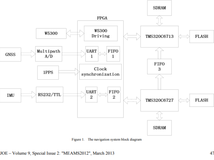
Integrated Navigation System, the navigation information processor needs to complete vast real-time data acquisition, processing and computing, including completing Inertial Measurement Unit (hereinafter referred to as the IMU) data acquisition and preprocessing, GNSS data preprocessing, clock signal synchronization, inertial system initial alignment, posture real-time update calculation, carrier motion parameter calculation, combined filtering and error online correction, etc., at the same time it shall also complete the data communication task between external sensors and equipments of the applied objects [4]. The navigation computer formed by a single DSP chip is difficult to meet the real-time demand of integrated navigation system therefore, the paper chooses two chips of TI company, i.e. TMS320C6727 (hereinafter referred to as C6727) and TMS320C6713 (hereinafter referred to as the C6713), to work in parallel. C6727 is responsible for IMU data acquisition, original data filtering and inertial navigation attitude update and calculation. C6713 is responsible for combined filtering and online error correction as well as exporting navigation results. IMU and GNSS data acquisition is realized by the FPGA to make the DSP chip FPGA focus on navigation calculating, thus greatly improves the real-time performance of the system and reduces power consumption of the system. The overall structure of the system is shown in Figure. 1.
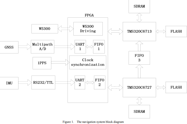
Embedded Integrated Navigation Computer introduced in the paper is divided into five modules, i.e. the data acquisition module, logic control module, navigation calculating module, navigation data output module. The data acquisition module is mainly composed of FPGA, RS232 shift TTL level switch chip MAX3232 and AD acquisition chip, is mainly used for receiving IMU output gyro, accelerometer, temperature information, and GNSS output navigation message information. Logic control module is mainly composed of FPGA structure, is used to decode the address of the two DSP chips for communication with peripheral chips, as well as external interrupt coding for read and discrimination of DSP interruption. IMU original data processing module is mainly composed of A/D converter, FPGA, C6727DSP, is mostly used for the output analog signals from gyro and accelerometer passing through the A/D converter chip and being converted into digital signals, then passing through the FIFO built inside the FPGA for data cache then being read into and filtered for de-noising by C6727DSP chip, then passing through FIFO to be output to C6713DSP. Navigation calculating module is mainly composed by C6713DSP, is mainly used to complete integrated navigation calculation. Navigation data output module is mainly composed of W5300 network card chip, and is mainly used to export navigation results to other applied equipment.
III. DATA ACQUISITION MOUDLE
The main functions of data acquisition module are: Acquisition of original gyro, accelerometer information exported from IMU at 200Hz; Receiving GNSS receiver output serial port message information; Receiving GNSS 1PPS pulse signal as the trigger signal for internal clock signal synchronization module; Receiving serial port information sent by the principal computer for FLASH solidification. Data acquisition module is mainly composed by level conversion chip and photoelectric coupling chipset, its working mode is: Put the IMU output digital signal into level conversion chip to convert it into TTL form of IMU signal, and then input it to the navigation information processing module through the EDMA. GNSS receiver output signal passing through the level conversion chip is converted into TTL level form of GNSS signal, and then input it to the navigation information processing module through the EDMA. GNSS’s 1 PPS (One Pulse Per Second) Second Pulse Signal passing through the photoelectric coupler is input to the clock synchronization module. The principal computer output solidification FLASH program signal passing through level conversion chip is converted into TTL form of digital signal, and then input it to the FLASH program solidification module in DSP through the EDMA.
IV. LOGIC CONTROL MOUDLE
The function of logic control module is: to realize control and management of the navigation information processor’s peripheral logic circuit through the FPGA chip. Logic control module is composed by FPGA and its configuration chip. The working mode is: FPGA realizes the Decoder module, Synchronization module, Universal Asynchronous Receiver/Transmitter (UART) module, Asynchronous FIFO (First In First Out) memory module and internet access chip driver module; And the FPGA configuration chip is used to store the configuration information of FPGA. Decoder module, Synchronization module, UART module and Internet Access chip driver module can be realized through the hardware description language (Verilog HDL) programming, Asynchronous FIFO storage module is realized by calling the Quartus Ⅱ IP soft core. As the hardware interface address of navigation information processor is mapped in DSP’s CE3 address space, so the Decoder module needs to decode corresponding high address of DSP, the decoding output serves as the Chip Selection signal of interface control chips. Synchronization module takes the inside signal and the outside signal as input, the external input is the 1PPS pulse signal from GNSS receiver, the internal input is the clock pulse signal generated by the internal clock circuit, the clock synchronization module is triggered by 1PPS signal rising edge, this synchronous mode is conducted 1 time/second to prevent phase shift for difference between the internal and external clock frequency. The UART module and the FIFO module implement conversion and storage of series/parallel data. The Internet Access Chip driver module implements initialization of the Internet Access Chip. V. NAVIGATION CALCUATION MODULE The function of navigation calculation module is: to operate inertial navigation’s initial alignment algorithm, strapdown calculating algorithm and SINS/GNSS integrated navigation algorithm through the DSP chips. Navigation calculating module includes DSP (TMS320C6713B), FLASH, SDRAM and other chips. Digital chips connect with external FLASH, SDRAM and FPGA chips through External Memory Interface (EMIF). DSP chips transfer data between external memory and peripherals through the Enhanced Direct Memory Access (EDMA) controller. GNSS digital signal and IMU digital signal are read by DSP chips through the EMIF interface, and then sent to the external SDRAM of DSP through the EDMA [5]. After navigation calculating is completed, the navigation data is sent to FPGA chip by EDMA through the EMIF interface. The working mode is: after the power is on, wait for the first frame of GNSS effective navigation data, GNSS input latitude, longitude and altitude and other initial position information into the navigation information processing board, after the navigation initial information becomes effective, the navigation module starts the initial alignment of Strapdown Inertial Navigation, then the Strapdown Inertial Navigation System begins to enter the Strapdown calculating model, uses the kalman filter to revise the navigation information exported by GNSS, and keeps a long time navigation accuracy.
VI. SYSTEM COMMUNICATION MODULE
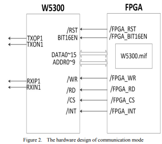
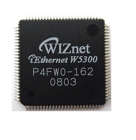
The function of navigation communication module is: to real-time send the navigation information obtained from navigation solution to other application equipments through the double redundancy Ethernet network interface. Navigation communication module is composed by FPGA chip and special Etheric Internet Access chip W5300. The W5300 is a 0.18 μm CMOS technology single chip into which 10/100 Ethernet controller, MAC, and TCP/IP are integrated. W5300 is designed for Internet embedded applications where easy implementation, stability, high performance, and effective cost are required. W5300's target application is the embedded internet solution requiring high performance such as multi-media streaming service. The Internet connectivity can be implemented easily and quickly only with single chip having TCP/IP protocol and 10/100 Ethernet MAC & PHY. The working mode is: network interface chip has a internal integration of 100M Ethernet controller, MAC and TCP/IP protocol stack. The data bus is connected with FPGA data bus, the network interface chip address line is completed by the FPGA internal address decoding module. The hardware design of navigation communication mode is show in Figure.2. The Etheric Internet Access chip W5300 register is need to be initialized when the chip begin to work. In this design, FPGA chip is chosen as the main control chip to realize the initialization of W5300. W5300 configuration information is stored in the W5300.mif file, which is stored in the ROM of the FPGA. After system power on, W5300.mif files will be written to the W5300 interior register by FPGA [6]. When DSP completes a navigation calculating, the address signal is decoded in FPGA internal address decoding module, thus selects the network interface chip CS signal, and then the navigation information through the network interface chip is converted into UDP mode network signal to be sent to other application equipments. Navigation data output mode adopts double-port network output, namely the MAC address along with the IP address, backup for each other; the two automatically switch working internet access according to the effectiveness of external equipment network interface to ensure the reliability of the network interface.
VII. CONCLUSION
The paper presents a SINS/GPS integrated navigation computer system based on double DSP and FPGA structure, describes in detail the use of FPGA to realize integrated navigation computer’s interface management and time sequence control design idea as well as using double DSP structure to complete the IMU original data acquisition and integrated navigation calculation flow operation idea. The design realizes the integrated navigation calculation’s embedded design, the design concept fully embodies the real-time information processing and real-time control phase separation, information distributed parallel processing design thought, hardware and software combined to realize the system’s target of high speed data acquisition and high speed information processing, satisfies the system’s requirements of small volume, high precision, high realtime performance, low power consumption etc., has practical engineering significance in the widely applications of integrated navigation system in low cost, low power consumption system areas.
ACKNOWLEDGMENT
The project was supported by following funds: National Natural Science Foundation of China (Nos. 51175082, 60904088, 61273056), Natural Science Foundation of Jiangsu Province (BK2012326), Open Research Fund of State Key Laboratory of Transient Optics and Photonics, Chinese Academy of Sciences (SKLST201108).