



How to Extend W5500 to Multiple Sockets on an Altera FPGA?
This project demonstrates a single-socket WIZnet W5500 interface implemented in Verilog for an Altera FPGA, using an SPI link described as operating at 80 MHz.
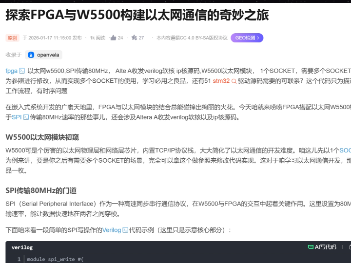
How to Extend W5500 to Multiple Sockets on an Altera FPGA?
Summary
This project demonstrates a single-socket WIZnet W5500 interface implemented in Verilog for an Altera FPGA, using an SPI link described as operating at 80 MHz. For an Industrial IoT design, the single-socket control flow can be extended into a multi-socket architecture by adding per-socket contexts, centralized SPI arbitration, shared buffer-transfer logic, and independent recovery timers. The W5500 remains responsible for Ethernet and TCP/IP processing, while the FPGA manages deterministic application data and socket scheduling.
What the Project Does
The source article presents an FPGA-to-W5500 Ethernet interface centered on a simplified Verilog SPI writer and a single W5500 socket. It describes the design as an Altera-oriented Verilog soft-core or IP-core resource that can be modified to support additional sockets. The author explicitly states that the example is intended to describe the W5500 workflow and contains timing problems, so it should be treated as instructional material rather than production-ready RTL.
The demonstrated architecture is approximately:
Industrial application logic → single-socket control logic → SPI write module → W5500 → Ethernet network
The SPI example accepts one byte, generates an SPI clock from the FPGA system clock, shifts the byte onto MOSI, controls chip select, and raises a completion flag after eight bits. The article does not provide a complete verified implementation of W5500 register framing, SPI reads, socket-buffer wraparound, simultaneous socket operation, or field-tested Industrial IoT communication.
A production multi-socket extension would use the following data path:
Sensors, control loops, or field interfaces → protocol-specific FIFOs → socket scheduler → W5500 register and buffer controller → shared SPI master → W5500 hardware sockets → Ethernet
The reverse path would move received socket data from the W5500 through the shared SPI master into socket-specific receive FIFOs and application logic.
Typical Industrial IoT socket assignments could include:
Cyclic process telemetry
Supervisory commands
Device configuration
Diagnostics and maintenance
Event or alarm reporting
DHCP or DNS support
Firmware-update transport
A reserved recovery or commissioning channel
The source does not implement or verify these assignments. They are an architecture-level extension of its stated single-socket design.
Where WIZnet Fits
The relevant WIZnet product is the W5500. It integrates a 10/100 Ethernet MAC and PHY, a hardwired TCP/IP engine, eight independent hardware sockets, and 32 KB of internal TX/RX memory. It communicates with a host through SPI modes 0 or 3 at up to 80 MHz.
Within the extended FPGA architecture, the W5500 performs:
Ethernet PHY and MAC operation
ARP and IPv4 processing
TCP and UDP socket-state handling
TCP acknowledgment and retransmission processing
Per-socket transmit and receive buffering
Link-status reporting
The Altera FPGA performs:
W5500 reset and configuration
SPI command generation
Socket allocation
Application-protocol framing
Transfer scheduling across sockets
FPGA FIFO management
Link and socket recovery
Industrial control and signal-processing functions
This division is useful when the FPGA must continue deterministic acquisition or control while network activity changes. Supported TCP/IP processing occurs inside the W5500 rather than being scheduled as software or implemented as a large collection of custom protocol state machines.
The design still has fixed resource constraints. All eight sockets share one SPI host interface and a total of 32 KB of W5500 packet memory. The FPGA must therefore schedule access and allocate buffer capacity according to application priority.
Implementation Notes
The source contains a short Verilog example rather than a downloadable, verified multi-socket codebase. Its own description warns that timing problems remain. The following excerpt is from the article’s inline SPI writer:
if (bit_counter == 3'd7) begin
    spi_cs_n    <= 1'b1;
    spi_wr_done <= 1'b1;
end else begin
    spi_cs_n    <= 1'b0;
    spi_mosi    <= data_to_send[7 - bit_counter];
    bit_counter <= bit_counter + 1;
end
This code exists to illustrate serializing one byte and reporting transfer completion. It does not by itself implement a valid complete W5500 transaction, because W5500 accesses also require an address phase, a control phase, read/write handling, and potentially a multi-byte data phase. The source also generates and then uses spi_clk as an internal clock, which requires careful timing analysis and is one reason the article’s warning about timing should be taken seriously.
Altera Integration Structure
A practical Altera implementation should divide the design into reusable modules.
Clock and reset block
Generate synchronous internal resets and hold the W5500 reset input active until the FPGA clock and supply are stable. A controlled W5500-only reset path should be available without resetting the industrial control logic.
SPI master
Implement a timing-clean SPI master referenced to the primary FPGA clock. Rather than creating an unconstrained internal clock and placing state logic directly on it, use a clock-enable architecture or a properly constrained generated clock.
The SPI master should support:
W5500 address and control headers
SPI read and write operations
Variable-length transfers
Continuous chip select during bursts
FIFO-based TX and RX streaming
Transfer completion
Timeout detection
Mode 0 or mode 3 timing
Programmable clock division
W5500 access controller
Translate logical requests into W5500 bus transactions. Higher-level modules should request operations such as:
Read common register
Write socket register
Read socket status
Write socket TX buffer
Read socket RX buffer
Update a socket pointer
Issue a socket command
This avoids duplicating the W5500 SPI framing logic in every socket controller.
Socket scheduler
Arbitrate requests from several socket contexts. One SPI transaction must complete before another socket is granted access.
A useful priority policy is:
RX service near buffer-full condition
Link and socket-state changes
Time-critical control traffic
Alarm traffic
Cyclic telemetry
Configuration and diagnostics
Background maintenance
Round-robin arbitration is simpler, but priority-aware scheduling is often more appropriate when control and diagnostic traffic have different deadlines.
Per-socket context
Each socket should retain its own state:
Protocol mode
Local port
Destination address and port
Current W5500 socket state
TX request length
RX available length
TX and RX pointer state
Timeout counter
Retry counter
Error flags
Application priority
The hardware context should not duplicate the complete SPI engine. All socket controllers should share the same lower-level W5500 access block.
Multi-Socket Initialization
At startup, the FPGA should:
Reset the W5500.
confirm stable register access.
Configure MAC, IPv4, subnet, and gateway values.
Allocate TX and RX memory to the required sockets.
Check the PHY link.
Configure each enabled socket.
Open or listen on sockets according to their assigned roles.
Report individual socket readiness to the application layer.
The W5500’s 32 KB memory is configurable per socket. Equal allocation is easy to understand but may be inefficient. An event socket carrying short alarm messages may need less memory than a firmware-update or continuous telemetry socket.
Multi-Socket Transmit Flow
For each pending transmit request:
The application places payload data into a socket-specific FIFO.
The socket context submits a request to the scheduler.
The scheduler grants ownership of the shared W5500 access controller.
The controller checks available TX memory.
It reads the socket TX write pointer.
It writes payload data into W5500 memory using SPI bursts.
It handles circular-buffer wraparound.
It updates the write pointer.
It issues the SEND command.
It releases the SPI engine while the socket waits for completion.
Waiting sockets should not block the SPI interface while another socket is waiting for a network event. The scheduler should interleave register polling and buffer transfers across active sockets.
Multi-Socket Receive Flow
For receive processing:
A W5500 interrupt or scheduled poll identifies an active socket.
The controller reads the socket receive-size register.
It reads the RX pointer.
It transfers data into the corresponding FPGA FIFO.
It handles buffer wraparound.
It updates the RX pointer.
It issues the receive-complete command.
It delivers data and metadata to the relevant application block.
TCP sockets must be treated as byte streams. UDP sockets must preserve datagram boundaries and extract the W5500 UDP source-address header before presenting the payload to the application.
Intel FPGA Tool Integration
In a modular Intel FPGA project, the custom W5500 controller can be packaged as an IP component and connected through Platform Designer. A register-controlled wrapper can expose configuration, status, interrupt, and FIFO interfaces through Avalon memory-mapped or streaming connections.
A pure-RTL system can connect application state machines directly to these interfaces. A hybrid system can expose the same W5500 controller to a Nios processor while leaving time-critical acquisition and transfer logic in hardware.
The source article only refers generally to Altera Verilog soft-core and IP-core material; it does not document a Platform Designer component, Avalon interface, Quartus project, timing constraints, or tested Intel FPGA device.
Direct RTL Versus an FPGA Soft-Core CPU
A soft-core alternative can place a Nios processor in the FPGA fabric. Intel’s Nios V is a RISC-V-based soft processor that runs application software and connects to FPGA peripherals through configurable system interconnects.
A direct-RTL architecture is:
Industrial logic → socket FSMs → shared W5500 controller → SPI → W5500
A soft-core architecture is:
Industrial logic → FIFO or Avalon interface → Nios software → SPI peripheral → W5500
Direct RTL provides:
Deterministic scheduling
No instruction or data memory requirement
Tight integration with FPGA datapaths
Low software dependence
Predictable fixed-function operation
It also creates:
More complex socket state machines
Greater RTL verification effort
More difficult feature changes
More complicated DHCP, DNS, configuration, and maintenance logic
A soft-core CPU provides:
C-based socket management
Easier reuse of WIZnet driver concepts
Simpler configuration and diagnostics
Easier protocol changes
More maintainable retry and recovery logic
It requires:
Processor logic resources
Instruction and data memory
A software toolchain
Firmware testing
Interrupt and scheduling analysis
For an Industrial IoT product, a hybrid architecture is often practical. RTL can handle deterministic sampling, timestamping, FIFO movement, and urgent socket scheduling, while the soft-core manages configuration, DHCP, DNS, diagnostics, firmware updates, and noncritical network services.
Practical Tips / Pitfalls
Treat the article’s SPI module as a workflow illustration, not reusable production IP. Its own author states that timing issues remain.
Do not duplicate one SPI master per socket. W5500 provides one shared SPI interface, so use centralized arbitration and per-socket contexts.
Constrain every generated clock or, preferably, implement SPI timing with clock enables in the primary FPGA clock domain.
Test circular-buffer wraparound separately for each configured TX and RX buffer size.
Apply a bounded timeout to every socket operation, SPI request, link wait, connection attempt, and transmission completion state.
Reserve socket and memory resources before defining application protocols; DHCP, DNS, maintenance, and diagnostics consume resources alongside production traffic.
Capture link-loss, socket-reset, SPI-timeout, buffer-overflow, and reconnect counters so failures can be diagnosed in the field.
FAQ
Q: Why use W5500 for a multi-socket Industrial IoT FPGA design?
W5500 supplies eight hardware sockets, 32 KB of packet memory, and hardwired TCP/IP processing. This allows the FPGA to focus on deterministic acquisition and control while avoiding a custom TCP/IP implementation in RTL. The main architectural challenge becomes scheduling one SPI interface across several socket contexts.
Q: How does W5500 connect to an Altera FPGA?
It connects through SPI using SCLK, MOSI, MISO, and chip select. Reset and interrupt signals should also be connected for controlled startup and event-driven processing. W5500 supports SPI modes 0 and 3 at up to 80 MHz, but actual timing must be verified through Quartus timing analysis and hardware measurements.
Q: What role does W5500 play in the multi-socket extension?
W5500 stores per-socket data, maintains TCP or UDP state, and processes supported Ethernet and TCP/IP operations. The FPGA decides which socket receives SPI service, transfers payloads, updates pointers, handles application framing, and applies recovery policy.
Q: Can beginners extend the single-socket example?
A basic two-socket extension is possible for developers familiar with Verilog FSMs, SPI, and W5500 registers. A reliable industrial implementation additionally requires arbitration, FIFO design, circular-buffer handling, timing constraints, asynchronous interrupt synchronization, socket recovery, and verification under concurrent traffic.
Q: How does direct RTL compare with a Nios soft-core CPU?
Direct RTL offers deterministic fixed-function behavior but turns network management into a hardware-verification task. A Nios soft-core consumes FPGA logic and memory but makes configuration, diagnostics, DHCP, retry logic, and changing protocols easier to implement in software. A hybrid design can keep deterministic data movement in RTL while assigning management functions to the processor.
Source
Original article: CSDN, Exploring Ethernet Communication with FPGA and W5500, published January 17, 2026. The article presents an 80 MHz SPI example, describes a single-socket Altera-oriented implementation, suggests multi-socket modification, and warns that its illustrative code has timing issues. It is published under CC BY-SA 4.0.
WIZnet technical reference: W5500 official product documentation and datasheet, covering eight sockets, 32 KB internal memory, hardwired TCP/IP protocols, integrated 10/100 MAC/PHY, and the SPI host interface.
Soft-core comparison reference: Intel Nios V processor documentation, describing a RISC-V soft processor instantiated in supported Intel FPGA fabric and integrated with FPGA peripherals and memory.
License: The CSDN article is marked CC BY-SA 4.0. No separate downloadable FPGA source package or independently verifiable RTL license was identified from the article.
Tags
#W5500 #WIZnet #AlteraFPGA #IntelFPGA #Verilog #MultiSocket #SPI #IndustrialIoT #Ethernet #NiosV #SoftCoreCPU #HardwareTCPIP
Altera FPGA에서 W5500을 다중 소켓으로 어떻게 확장할 수 있을까?
요약
이 프로젝트는 Altera FPGA에서 Verilog로 구현된 단일 소켓 WIZnet W5500 인터페이스를 다루며, 최대 80 MHz로 설명된 SPI 연결을 사용합니다. 산업용 IoT 설계에서는 소켓별 컨텍스트, 중앙 집중식 SPI 중재, 공유 버퍼 전송 로직, 독립적인 복구 타이머를 추가해 단일 소켓 제어 흐름을 다중 소켓 구조로 확장할 수 있습니다. W5500은 이더넷과 TCP/IP 처리를 담당하고, FPGA는 결정론적인 애플리케이션 데이터 처리와 소켓 스케줄링을 수행합니다.
프로젝트가 하는 일
원문은 단순화된 Verilog SPI 쓰기 모듈과 하나의 W5500 소켓을 중심으로 FPGA와 W5500 사이의 이더넷 인터페이스를 설명합니다. 설계는 Altera FPGA용 Verilog 소프트 코어 또는 IP 코어 자료로 소개되며, 추가 소켓을 지원하도록 수정할 수 있다고 설명합니다.
원문 작성자는 이 코드가 W5500의 동작 흐름을 설명하기 위한 예제이며 타이밍 문제가 남아 있다고 명시합니다. 따라서 이를 양산 가능한 RTL로 보기보다는 학습 및 구조 이해를 위한 자료로 취급해야 합니다.
원문이 제시하는 기본 구조는 대략 다음과 같습니다.
산업용 애플리케이션 로직 → 단일 소켓 제어 로직 → SPI 쓰기 모듈 → W5500 → 이더넷 네트워크
SPI 예제는 1바이트 데이터를 입력받아 FPGA 시스템 클럭으로 SPI 클럭을 생성하고, MOSI로 데이터를 직렬 전송하며, 칩 선택 신호를 제어하고, 8비트 전송이 끝나면 완료 플래그를 출력합니다.
그러나 원문은 다음 기능을 포함하는 완성된 구현을 제공하지 않습니다.
전체 W5500 레지스터 프레임 생성
SPI 읽기 동작
소켓 버퍼 원형 래핑
여러 소켓의 동시 처리
산업 현장에서 검증된 통신 로직
양산용 다중 소켓 확장 구조는 다음과 같은 데이터 경로를 사용할 수 있습니다.
센서, 제어 루프 또는 필드 인터페이스 → 프로토콜별 FIFO → 소켓 스케줄러 → W5500 레지스터 및 버퍼 컨트롤러 → 공유 SPI 마스터 → W5500 하드웨어 소켓 → 이더넷
수신 경로에서는 W5500의 소켓별 데이터를 공유 SPI 마스터를 통해 읽고, 각 소켓 전용 수신 FIFO와 애플리케이션 로직으로 전달합니다.
산업용 IoT 환경에서는 소켓을 다음과 같이 배정할 수 있습니다.
주기적인 공정 텔레메트리
감독 제어 명령
장치 설정
진단 및 유지보수
이벤트 또는 알람 보고
DHCP 또는 DNS
펌웨어 업데이트
복구 또는 현장 설정용 예비 채널
이러한 소켓 배정은 원문에서 구현된 내용이 아니라, 단일 소켓 구조를 산업용 다중 소켓 시스템으로 확장한 아키텍처 제안입니다.
WIZnet이 적용되는 위치
사용되는 제품은 WIZnet W5500입니다. W5500은 10/100 이더넷 MAC과 PHY, 하드와이어드 TCP/IP 엔진, 8개의 독립적인 하드웨어 소켓, 32 KB의 내부 TX/RX 메모리를 통합합니다. 호스트와는 SPI 모드 0 또는 모드 3으로 연결되며 최대 80 MHz로 동작할 수 있습니다.
확장된 FPGA 아키텍처에서 W5500은 다음 기능을 수행합니다.
이더넷 PHY 및 MAC 동작
ARP 및 IPv4 처리
TCP 및 UDP 소켓 상태 관리
TCP 확인 응답과 재전송 처리
소켓별 송수신 버퍼링
링크 상태 보고
Altera FPGA는 다음 기능을 수행합니다.
W5500 리셋 및 설정
SPI 명령 생성
소켓 할당
애플리케이션 프로토콜 프레이밍
소켓 간 전송 스케줄링
FPGA FIFO 관리
링크 및 소켓 복구
산업 제어 및 신호 처리
이러한 역할 분담은 네트워크 트래픽이 변하더라도 FPGA가 결정론적인 데이터 수집과 제어를 계속 수행해야 하는 환경에서 유용합니다. 지원되는 TCP/IP 처리는 FPGA의 소프트웨어나 대규모 사용자 정의 프로토콜 상태 머신이 아니라 W5500 내부에서 처리됩니다.
그러나 자원은 고정되어 있습니다. 8개의 모든 소켓은 하나의 SPI 호스트 인터페이스와 총 32 KB의 W5500 패킷 메모리를 공유합니다. 따라서 FPGA는 애플리케이션 우선순위에 따라 SPI 접근을 스케줄링하고 버퍼를 배분해야 합니다.
구현 참고 사항
원문은 다운로드 가능한 검증된 다중 소켓 코드베이스가 아니라 짧은 Verilog 예제를 제공합니다. 원문 자체에서도 타이밍 문제가 남아 있다고 설명합니다.
다음 코드는 원문에 포함된 SPI 쓰기 로직의 일부입니다.
if (bit_counter == 3'd7) begin
    spi_cs_n    <= 1'b1;
    spi_wr_done <= 1'b1;
end else begin
    spi_cs_n    <= 1'b0;
    spi_mosi    <= data_to_send[7 - bit_counter];
    bit_counter <= bit_counter + 1;
end
이 코드는 1바이트를 직렬화하고 전송 완료 상태를 출력하는 흐름을 설명하기 위해 존재합니다.
그러나 이 코드만으로는 완전한 W5500 트랜잭션을 구현할 수 없습니다. W5500 접근에는 주소 단계, 제어 단계, 읽기 또는 쓰기 처리, 선택적인 다중 바이트 데이터 단계가 필요합니다.
또한 원문 예제는 spi_clk를 내부에서 생성한 뒤 이를 다시 상태 로직의 클럭처럼 사용하는 구조를 설명합니다. 이 방식은 신중한 타이밍 분석이 필요하며, 원문에서 타이밍 문제가 있다고 경고한 이유 중 하나로 볼 수 있습니다.
Altera 통합 구조
실용적인 Altera FPGA 구현은 다음과 같은 재사용 가능한 모듈로 분리하는 것이 좋습니다.
클럭 및 리셋 블록
내부 리셋을 동기식으로 생성하고, FPGA 클럭과 전원 공급이 안정될 때까지 W5500 리셋 입력을 활성 상태로 유지합니다.
산업 제어 로직 전체를 재시작하지 않고 W5500만 재초기화할 수 있는 별도의 리셋 경로도 제공해야 합니다.
SPI 마스터
SPI 마스터는 FPGA의 주 클럭을 기준으로 타이밍이 명확한 구조로 구현해야 합니다.
제약이 없는 내부 클럭을 생성해 상태 로직을 직접 구동하기보다는, 주 클럭 도메인에서 clock enable 방식으로 SPI 타이밍을 생성하거나 적절히 제약된 generated clock을 사용하는 것이 좋습니다.
SPI 마스터는 다음 기능을 지원해야 합니다.
W5500 주소 및 제어 헤더
SPI 읽기 및 쓰기
가변 길이 전송
버스트 전송 중 연속 칩 선택
FIFO 기반 TX/RX 스트리밍
전송 완료 표시
타임아웃 감지
SPI 모드 0 또는 모드 3
설정 가능한 클럭 분주
W5500 접근 컨트롤러
이 모듈은 논리적인 요청을 실제 W5500 SPI 트랜잭션으로 변환합니다.
상위 모듈은 다음과 같은 추상화된 요청을 사용할 수 있습니다.
공통 레지스터 읽기
소켓 레지스터 쓰기
소켓 상태 읽기
소켓 TX 버퍼 쓰기
소켓 RX 버퍼 읽기
소켓 포인터 갱신
소켓 명령 실행
이 구조를 사용하면 각 소켓 컨트롤러가 W5500 SPI 프레임 형식을 중복 구현하지 않아도 됩니다.
소켓 스케줄러
여러 소켓 컨텍스트의 요청을 중재합니다. 하나의 SPI 트랜잭션이 끝나기 전에 다른 소켓이 SPI 버스를 사용할 수 없습니다.
산업용 시스템에서는 다음과 같은 우선순위를 적용할 수 있습니다.
버퍼 가득 참에 가까운 RX 처리
링크 및 소켓 상태 변화
시간 민감도가 높은 제어 트래픽
알람 트래픽
주기적 텔레메트리
설정 및 진단
백그라운드 유지보수
라운드 로빈 방식은 구현이 단순하지만, 제어 트래픽과 진단 트래픽의 마감 시간이 다른 경우에는 우선순위 기반 스케줄링이 더 적절할 수 있습니다.
소켓별 컨텍스트
각 소켓은 다음 상태를 독립적으로 유지해야 합니다.
프로토콜 모드
로컬 포트
목적지 IP 주소 및 포트
현재 W5500 소켓 상태
TX 요청 길이
사용 가능한 RX 데이터 길이
TX/RX 포인터 상태
타임아웃 카운터
재시도 카운터
오류 플래그
애플리케이션 우선순위
소켓별로 완전한 SPI 엔진을 복제해서는 안 됩니다. 모든 소켓 컨트롤러가 하나의 하위 W5500 접근 블록을 공유해야 합니다.
다중 소켓 초기화
시작 시 FPGA는 다음 순서를 수행할 수 있습니다.
W5500을 리셋합니다.
레지스터 접근이 안정적인지 확인합니다.
MAC 주소, IPv4 주소, 서브넷 마스크, 게이트웨이를 설정합니다.
필요한 소켓에 TX/RX 메모리를 할당합니다.
PHY 링크를 확인합니다.
활성화할 각 소켓을 설정합니다.
역할에 따라 소켓을 열거나 LISTEN 상태로 전환합니다.
각 소켓의 준비 상태를 애플리케이션 계층에 보고합니다.
W5500의 32 KB 메모리는 소켓별로 할당할 수 있습니다. 동일한 크기로 배분하면 이해하기 쉽지만 비효율적일 수 있습니다.
짧은 알람 메시지만 보내는 이벤트 소켓은 적은 메모리로 충분할 수 있고, 펌웨어 업데이트나 연속 텔레메트리 소켓은 더 큰 버퍼가 필요할 수 있습니다.
다중 소켓 송신 흐름
각 송신 요청은 다음 순서로 처리할 수 있습니다.
애플리케이션이 페이로드를 소켓별 FIFO에 기록합니다.
소켓 컨텍스트가 스케줄러에 서비스를 요청합니다.
스케줄러가 공유 W5500 접근 컨트롤러의 사용 권한을 부여합니다.
컨트롤러가 사용 가능한 TX 메모리를 확인합니다.
소켓 TX 쓰기 포인터를 읽습니다.
SPI 버스트를 사용해 W5500 메모리에 페이로드를 기록합니다.
원형 버퍼 래핑을 처리합니다.
쓰기 포인터를 갱신합니다.
SEND 명령을 실행합니다.
소켓이 전송 완료를 기다리는 동안 SPI 엔진 사용 권한을 해제합니다.
한 소켓이 네트워크 이벤트를 기다리는 동안 SPI 인터페이스를 계속 점유해서는 안 됩니다. 스케줄러는 여러 활성 소켓의 레지스터 폴링과 버퍼 전송을 번갈아 처리해야 합니다.
다중 소켓 수신 흐름
수신 처리는 다음과 같이 구성할 수 있습니다.
W5500 인터럽트 또는 주기적 폴링으로 활성 소켓을 확인합니다.
소켓 수신 크기 레지스터를 읽습니다.
RX 포인터를 읽습니다.
데이터를 해당 FPGA FIFO로 전송합니다.
원형 버퍼 래핑을 처리합니다.
RX 포인터를 갱신합니다.
수신 완료 명령을 실행합니다.
데이터와 메타데이터를 관련 애플리케이션 블록에 전달합니다.
TCP 소켓은 바이트 스트림으로 처리해야 합니다. UDP 소켓은 데이터그램 경계를 유지하고, W5500이 추가하는 UDP 송신자 주소 헤더를 제거한 뒤 페이로드를 애플리케이션에 전달해야 합니다.
Intel FPGA 도구 통합
모듈형 Intel FPGA 프로젝트에서는 사용자 정의 W5500 컨트롤러를 IP 컴포넌트로 패키징한 뒤 Platform Designer에 연결할 수 있습니다.
레지스터 기반 래퍼는 Avalon Memory-Mapped 또는 Avalon Streaming 인터페이스를 통해 다음 기능을 노출할 수 있습니다.
설정 레지스터
상태 레지스터
인터럽트
송수신 FIFO
오류 카운터
소켓 상태
순수 RTL 시스템에서는 애플리케이션 FSM을 이러한 인터페이스에 직접 연결할 수 있습니다.
혼합형 시스템에서는 동일한 W5500 컨트롤러를 Nios 프로세서에 연결하고, 시간 민감도가 높은 데이터 수집과 전송 로직은 하드웨어에 유지할 수 있습니다.
원문은 Altera용 Verilog 소프트 코어와 IP 코어 자료를 일반적으로 언급할 뿐, Platform Designer 컴포넌트, Avalon 인터페이스, Quartus 프로젝트, 타이밍 제약, 검증된 Intel FPGA 디바이스를 문서화하지는 않습니다.
직접 RTL과 FPGA 소프트 코어 CPU 비교
소프트 코어 대안으로는 FPGA 패브릭 내부에 Nios 프로세서를 배치할 수 있습니다. Intel Nios V는 RISC-V 기반 소프트 프로세서로, 소프트웨어를 실행하고 FPGA 주변장치 및 메모리와 연결할 수 있습니다.
직접 RTL 구조는 다음과 같습니다.
산업용 로직 → 소켓 FSM → 공유 W5500 컨트롤러 → SPI → W5500
소프트 코어 구조는 다음과 같습니다.
산업용 로직 → FIFO 또는 Avalon 인터페이스 → Nios 소프트웨어 → SPI 주변장치 → W5500
직접 RTL 방식의 장점은 다음과 같습니다.
결정론적인 스케줄링
명령 메모리 및 데이터 메모리 불필요
FPGA 데이터 경로와 긴밀한 결합
낮은 소프트웨어 의존성
예측 가능한 고정 기능 동작
반면 다음과 같은 부담이 있습니다.
더 복잡한 소켓 상태 머신
더 높은 RTL 검증 비용
기능 변경의 어려움
DHCP, DNS, 설정, 유지보수 로직 구현의 복잡성
소프트 코어 CPU의 장점은 다음과 같습니다.
C 기반 소켓 관리
WIZnet 드라이버 개념의 쉬운 재사용
단순한 설정 및 진단
쉬운 프로토콜 변경
재시도 및 복구 로직의 유지보수성
그러나 다음 자원이 추가로 필요합니다.
프로세서 논리 자원
명령 및 데이터 메모리
소프트웨어 툴체인
펌웨어 시험
인터럽트 및 스케줄링 분석
산업용 IoT 제품에서는 혼합형 아키텍처가 실용적일 수 있습니다. RTL은 결정론적인 샘플링, 타임스탬프, FIFO 이동, 긴급 소켓 스케줄링을 담당하고, 소프트 코어는 설정, DHCP, DNS, 진단, 펌웨어 업데이트, 비실시간 네트워크 서비스를 담당할 수 있습니다.
실무 팁과 주의사항
원문의 SPI 모듈은 동작 흐름을 설명하는 예제로 사용해야 하며, 그대로 양산 IP로 재사용해서는 안 됩니다. 원문 작성자도 타이밍 문제가 남아 있다고 명시합니다.
소켓마다 SPI 마스터를 하나씩 복제해서는 안 됩니다. W5500은 하나의 SPI 인터페이스만 제공하므로 중앙 중재와 소켓별 컨텍스트를 사용해야 합니다.
모든 generated clock에 제약을 적용해야 하며, 가능하면 주 FPGA 클럭 도메인에서 clock enable 방식으로 SPI 타이밍을 구현하는 것이 좋습니다.
설정한 각 TX/RX 버퍼 크기에 대해 원형 버퍼 래핑을 별도로 시험해야 합니다.
모든 소켓 동작, SPI 요청, 링크 대기, 연결 시도, 전송 완료 상태에 제한된 타임아웃을 적용해야 합니다.
애플리케이션 프로토콜을 확정하기 전에 소켓과 메모리 자원을 먼저 배정해야 합니다. DHCP, DNS, 유지보수, 진단도 운영 트래픽과 동일한 자원을 사용합니다.
링크 손실, 소켓 리셋, SPI 타임아웃, 버퍼 오버플로, 재연결 횟수를 기록해야 현장 장애를 분석할 수 있습니다.
FAQ
Q: 다중 소켓 산업용 IoT FPGA 설계에서 W5500을 사용하는 이유는 무엇인가요?
W5500은 8개의 하드웨어 소켓, 32 KB 패킷 메모리, 하드와이어드 TCP/IP 처리를 제공합니다. 이를 통해 FPGA는 사용자 정의 TCP/IP 스택을 RTL로 구현하지 않고도 결정론적인 데이터 수집과 제어에 집중할 수 있습니다. 핵심 아키텍처 과제는 여러 소켓이 하나의 SPI 인터페이스를 공유하도록 스케줄링하는 것입니다.
Q: W5500은 Altera FPGA와 어떻게 연결하나요?
SCLK, MOSI, MISO, 칩 선택 신호를 사용하는 SPI로 연결합니다. 제어된 시작과 이벤트 기반 처리를 위해 리셋과 인터럽트 신호도 연결하는 것이 좋습니다. W5500은 SPI 모드 0과 모드 3에서 최대 80 MHz를 지원하지만, 실제 타이밍은 Quartus 타이밍 분석과 하드웨어 측정을 통해 검증해야 합니다.
Q: 다중 소켓 확장에서 W5500은 어떤 역할을 하나요?
W5500은 소켓별 데이터를 저장하고 TCP 또는 UDP 상태를 유지하며, 지원되는 이더넷과 TCP/IP 동작을 처리합니다. FPGA는 어떤 소켓이 SPI 서비스를 받을지 결정하고, 페이로드를 전송하며, 포인터를 갱신하고, 애플리케이션 프레이밍과 복구 정책을 적용합니다.
Q: 초보자도 단일 소켓 예제를 확장할 수 있나요?
Verilog FSM, SPI, W5500 레지스터에 익숙하다면 기본적인 2소켓 확장은 가능합니다. 그러나 산업용으로 신뢰성 있게 구현하려면 중재, FIFO 설계, 원형 버퍼 처리, 타이밍 제약, 비동기 인터럽트 동기화, 소켓 복구, 동시 트래픽 검증이 필요합니다.
Q: 직접 RTL 구현은 Nios 소프트 코어 CPU와 어떻게 다른가요?
직접 RTL은 결정론적인 고정 기능 동작을 제공하지만 네트워크 관리가 하드웨어 검증 문제로 바뀝니다. Nios 소프트 코어는 FPGA 논리와 메모리를 추가로 사용하지만 설정, 진단, DHCP, 재시도, 변경되는 프로토콜을 소프트웨어로 구현하기 쉽습니다. 혼합형 구조에서는 결정론적인 데이터 이동은 RTL이 처리하고 관리 기능은 프로세서가 담당할 수 있습니다.
출처
원문: CSDN, FPGA와 W5500을 이용한 이더넷 통신 분석
https://blog.csdn.net/qq__487739278/article/details/157028894
원문은 2026년 1월 17일 게시된 것으로 표시되며, 80 MHz SPI 예제와 단일 소켓 Altera 기반 구현을 설명합니다. 다중 소켓 확장 가능성을 언급하면서도, 예제 코드에 타이밍 문제가 있다고 명시합니다. 라이선스는 CC BY-SA 4.0으로 표시됩니다.
WIZnet 기술 참고 자료: W5500 공식 제품 문서 및 데이터시트
https://docs.wiznet.io/Product/Chip/Ethernet/W5500
W5500의 8개 소켓, 32 KB 내부 메모리, 하드와이어드 TCP/IP 프로토콜, 통합 10/100 MAC/PHY, SPI 호스트 인터페이스를 설명합니다.
소프트 코어 비교 참고 자료: Intel Nios V 프로세서 문서
Nios V가 Intel FPGA 패브릭에 구현되는 RISC-V 기반 소프트 프로세서이며, FPGA 주변장치 및 메모리와 연결되는 구조를 설명합니다.
라이선스: CSDN 원문은 CC BY-SA 4.0으로 표시됩니다. 별도의 다운로드 가능한 FPGA 소스 패키지나 독립적으로 검증 가능한 RTL 라이선스는 원문에서 확인되지 않았습니다.
태그
#W5500 #WIZnet #AlteraFPGA #IntelFPGA #Verilog #MultiSocket #SPI #IndustrialIoT #Ethernet #NiosV #SoftCoreCPU #HardwareTCPIP