



How to Build an 80 MHz SPI TCP Client with WIZnet W5500 on FPGA?
This education-focused project uses Verilog FPGA logic to control a WIZnet W5500 as a multi-socket TCP client.
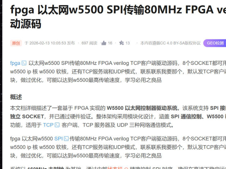
How to Build an 80 MHz SPI TCP Client with WIZnet W5500 on FPGA?
Summary
This education-focused project uses Verilog FPGA logic to control a WIZnet W5500 as a multi-socket TCP client. The source describes a 160 MHz FPGA system clock, an 80 MHz W5500 SPI clock, support for all eight hardware sockets, and state-machine-based initialization, interrupt polling, transmission, and reception. W5500 provides the Ethernet MAC/PHY, hardwired TCP/IP processing, socket state machines, retransmission handling, and 32 KB packet memory. The FPGA implements the host-side SPI controller, register sequencer, socket scheduler, buffer movement, and application data interface. The article states that the design was tested in hardware, but it does not expose inspectable Verilog source or reproducible throughput measurements.
What the Project Does
The project implements the W5500 host driver entirely in FPGA logic rather than running a software driver on a microcontroller. Its default configuration is presented as a TCP client, while the source also mentions separate TCP server and UDP variants.
The system-level data path is:
FPGA application logic → transmit FIFO → socket scheduler → W5500 register and buffer controller → 80 MHz SPI master → W5500 → Ethernet network → TCP server
The receive path operates in reverse:
TCP server → Ethernet network → W5500 socket Rx buffer → SPI read controller → receive FIFO → FPGA application logic
The source describes five principal functional blocks:
An SPI subsystem that generates SCLK, controls chip select, and serializes register and payload data.
A W5500 initialization block that configures common and socket registers.
An interrupt-status block that polls W5500 interrupt registers.
A read/write controller that transfers payloads between FPGA logic and W5500 buffers.
A top-level coordinator that sequences initialization, event polling, transmission, and reception.
For education, this architecture exposes the complete boundary between an FPGA application and a hardware TCP/IP controller. Students can examine SPI timing, finite-state-machine sequencing, register maps, circular buffer pointers, socket state transitions, and the difference between raw interface clock rate and useful network throughput.
Where WIZnet Fits
The exact WIZnet product is W5500. It sits between the FPGA data path and the physical Ethernet network.
W5500 integrates:
A 10/100 Ethernet MAC and PHY
A hardwired IPv4 TCP/IP stack
Eight independent hardware sockets
32 KB of internal Tx/Rx memory
TCP, UDP, ICMP, ARP, IGMP, IPv4, and PPPoE processing
An SPI host interface supporting modes 0 and 3 at up to 80 MHz
The FPGA remains responsible for configuring and operating those resources. It must write the network identity, initialize sockets, transfer payloads, maintain buffer pointers, inspect interrupt causes, and recover failed connections.
The source assigns 2 KB of Tx memory and 2 KB of Rx memory to each of the eight sockets. This evenly divides W5500’s available packet memory and simplifies multi-socket teaching, although a production design could allocate memory unevenly when some connections carry substantially more traffic than others.
W5500 handles TCP connection state and retransmission internally, but it does not define the FPGA application protocol. The FPGA must still determine message boundaries, packet contents, queue policy, command validation, and how received data affects the rest of the hardware design.
Implementation Notes
The CSDN article describes Verilog source code but does not expose inspectable HDL modules in the accessible page. Project-specific signal names, finite-state encodings, timing constraints, FPGA resource use, and measured throughput therefore cannot be quoted or independently confirmed. The following notes describe the architecture supported by the visible source and official W5500 documentation.
Clock and SPI architecture
The source uses a 160 MHz FPGA clock to generate an 80 MHz W5500 SCLK. MOSI changes on the falling edge, and MISO is sampled on the rising edge, corresponding to W5500 SPI mode 0 behavior. WIZnet documentation confirms that W5500 accepts data on the rising edge and changes output data on the falling edge in both supported SPI modes.
A practical SPI state machine should support:
Common-register reads and writes
Socket-register reads and writes
Variable-length Tx-buffer writes
Variable-length Rx-buffer reads
Transaction completion and timeout outputs
Burst transfers without unnecessary chip-select toggling
The source describes fixed-length operations for small register accesses and variable-length operations for payload transfers. That separation is important because repeated short SPI transactions introduce proportionally more address, control-byte, and chip-select overhead.
Initialization sequence
The source’s initialization block performs hardware reset, checks physical-link state, and programs the following common registers:
SIPR for the local IP address
SUBR for the subnet mask
GAR for the gateway address
SHAR for the MAC address
RTR for retransmission timeout
RCR for retransmission count
Each active socket then receives its buffer allocation, source port, destination IP, destination port, and operating mode. The controller writes Sn_MR, issues OPEN, and proceeds to CONNECT for TCP-client operation.
A classroom implementation should additionally read W5500’s version register before socket initialization. This separates basic SPI and reset failures from later IP, link, or TCP-state problems.
Event handling
The source polls SIR to identify the socket that generated an event and then reads that socket’s Sn_IR. It interprets events such as connection establishment, disconnection, received data, transmission completion, and timeout, then clears the event by writing the corresponding status bits back to Sn_IR.
Polling avoids dependence on the external interrupt pin and makes the design easier to move between FPGA boards. The trade-off is that polling consumes SPI bandwidth and creates a service delay determined by the scan interval and number of sockets.
An educational design should measure:
Complete eight-socket polling time
Delay from packet arrival to Rx-buffer service
SPI bandwidth consumed by status reads
Event latency while a large payload transfer is active
Transmit path
The source describes the following transmit sequence:
Read Sn_TX_WR.
Write the payload into the selected socket’s Tx buffer.
Advance and write back Sn_TX_WR.
Write SEND to Sn_CR.
Poll for the send-complete or timeout event.
A robust implementation should also check available Tx space before beginning the payload transfer. The transmit controller needs to handle circular-buffer wraparound and prevent a new request from overwriting a transfer that has not completed.
Receive path
The receive sequence described by the source is:
Detect the receive event.
Read Sn_RX_RSR to determine the available byte count.
Read Sn_RX_RD to locate the current data.
Transfer the payload from W5500 memory to an FPGA FIFO.
Advance and write back Sn_RX_RD.
Issue RECV so W5500 can release the consumed buffer area.
The FPGA FIFO must be large enough for the selected service interval and packet pattern. If downstream logic cannot accept data, the design needs explicit backpressure, packet-drop, or socket-reset behavior.
Performance interpretation
An 80 MHz SPI clock is the maximum supported host-interface clock, not a guarantee of 80 Mbps application throughput. Each network transfer also requires address and control phases, register reads, pointer updates, socket commands, event polling, TCP/IP and Ethernet headers, acknowledgements, and FPGA scheduling.
The source claims optimization toward W5500’s maximum transfer speed but provides no packet size, test endpoint, TCP-window behavior, elapsed time, retransmission count, or measured Mbps result. Its performance claim should therefore be treated as an implementation objective rather than a reproducible benchmark.
WIZnet’s own published SPI performance examples demonstrate that measured throughput changes with host architecture, SPI frequency, application buffer size, socket-buffer allocation, and test conditions. Those MCU results are not benchmarks for this FPGA implementation, but they confirm that SPI clock alone is insufficient to predict application throughput.
Practical Tips / Pitfalls
Verify reset, SPI mode, and the W5500 version register at a conservative clock before enabling 80 MHz operation.
Constrain SCLK, MOSI, MISO, and chip-select timing explicitly in the FPGA project and verify them after place-and-route.
Use burst payload transfers; repeated single-byte transactions waste SPI bandwidth on address and control phases.
Measure the cost of polling all eight sockets, especially while long Tx or Rx transfers are active.
Handle Tx and Rx pointer wraparound explicitly and test transfers that cross a socket-buffer boundary.
Add counters for SPI timeout, TCP timeout, disconnect, FIFO overflow, send completion, retransmission, and socket recovery.
Benchmark with defined payload sizes, socket counts, traffic directions, test durations, and loss conditions rather than reporting only the SPI clock.
FAQ
Q: Why use WIZnet W5500 for an FPGA TCP-client project?
A: W5500 removes the need to implement an Ethernet MAC, PHY interface, ARP, IPv4, TCP state machine, and retransmission engine in FPGA logic. The FPGA instead operates a defined SPI register and buffer interface while retaining control of socket scheduling, payload movement, and application behavior. W5500’s eight sockets and internal packet memory also make multi-connection experiments possible without storing every Ethernet packet in FPGA block RAM.
Q: How does W5500 connect to the FPGA?
A: The host interface uses SCLK, MOSI, MISO, and chip select, together with reset and optionally the W5500 interrupt output. The source generates an 80 MHz SCLK from a 160 MHz FPGA clock and uses mode-0 edge timing. The Ethernet side is handled by W5500’s integrated MAC and PHY through the board’s magnetics and RJ45 interface.
Q: What role does W5500 play in this design?
A: W5500 manages the physical Ethernet link, IPv4 processing, TCP connection state, retransmission, socket status, and packet buffers. The FPGA configures W5500, selects sockets, transfers data through SPI, responds to events, and connects received or transmitted payloads to the rest of the hardware system.
Q: Can beginners follow this project?
A: It is appropriate for students who already understand basic Verilog, synchronous finite-state machines, FIFOs, SPI, and simulation. A practical learning sequence is version-register access, network-register initialization, PHY-link checking, one TCP socket, payload transmission, payload reception, interrupt polling, and finally eight-socket scheduling.
Q: Does an 80 MHz SPI clock mean the TCP client transfers 80 Mbps?
A: No. The SPI clock describes raw serial-interface timing. Useful TCP throughput is lower because the bus also carries W5500 addresses, control bytes, register operations, pointer updates, event polling, and socket commands. Network headers, acknowledgements, retransmissions, payload size, and server behavior also affect the result. The source gives no reproducible Mbps measurement, so throughput must be measured on the actual FPGA board.
Source
Original article: CSDN, “fpga 以太网w5500 SPI传输80MHz FPGA verilog TCP客户端驱动源码.” The article describes an FPGA-based W5500 controller using a 160 MHz system clock, an 80 MHz SPI interface, eight sockets, TCP-client operation, initialization logic, interrupt polling, and Tx/Rx controllers. It states that the implementation passed hardware testing but does not provide inspectable Verilog source or reproducible throughput results on the accessible page. The article is published under CC 4.0 BY-SA.
WIZnet product reference: Official W5500 documentation and datasheet covering the hardwired TCP/IP stack, eight sockets, 32 KB packet memory, 10/100 Ethernet MAC/PHY, supported protocols, and SPI operation up to 80 MHz.
Performance reference: WIZnet’s published W5500 SPI performance examples, showing the effect of host platform, SPI frequency, buffer size, and socket allocation on measured throughput. The published MCU tests are methodological references and are not measurements of the FPGA design described in the source article.
Register and software reference: WIZnet ioLibrary_Driver, an MIT-licensed reference for W5500 register access, socket behavior, and application integration. It is not confirmed as the source of the article’s Verilog implementation.
Tags
#W5500 #WIZnet #FPGA #Verilog #TCPClient #SPI80MHz #Ethernet #Education #MultiSocket #HardwareNetworking
FPGA에서 WIZnet W5500으로 80MHz SPI TCP Client를 구축하는 방법은?
요약
이 교육 중심 프로젝트는 Verilog FPGA logic으로 WIZnet W5500을 제어해 multi-socket TCP client를 구현합니다. 원본 자료는 160MHz FPGA system clock, 80MHz W5500 SPI clock, 8개 hardware socket 전체 지원, state machine 기반 initialization, interrupt polling, transmission, reception 구조를 설명합니다. W5500은 Ethernet MAC/PHY, hardwired TCP/IP processing, socket state machine, retransmission handling, 32KB packet memory를 제공합니다. FPGA는 host-side SPI controller, register sequencer, socket scheduler, buffer movement, application data interface를 구현합니다. 원본 글은 hardware test를 통과했다고 설명하지만, 검토 가능한 Verilog source나 재현 가능한 throughput 측정값은 공개하지 않습니다.
프로젝트가 하는 일
이 프로젝트는 microcontroller에서 software driver를 실행하는 대신 W5500 host driver 전체를 FPGA logic으로 구현합니다. 기본 configuration은 TCP client이며, 원본 자료에서는 별도의 TCP server 및 UDP version도 언급합니다.
System-level data path는 다음과 같습니다.
FPGA application logic → transmit FIFO → socket scheduler → W5500 register and buffer controller → 80MHz SPI master → W5500 → Ethernet network → TCP server
수신 경로는 반대 방향으로 동작합니다.
TCP server → Ethernet network → W5500 socket Rx buffer → SPI read controller → receive FIFO → FPGA application logic
원본 자료는 다음 5개의 주요 functional block을 설명합니다.
SCLK 생성, chip select 제어, register 및 payload data 직렬화를 담당하는 SPI subsystem
Common register와 socket register를 설정하는 W5500 initialization block
W5500 interrupt register를 polling하는 interrupt-status block
FPGA logic과 W5500 buffer 사이에서 payload를 이동하는 read/write controller
Initialization, event polling, transmission, reception을 순차적으로 제어하는 top-level coordinator
교육 측면에서 이 architecture는 FPGA application과 hardware TCP/IP controller 사이의 전체 경계를 보여줍니다. 학생은 SPI timing, finite-state-machine sequencing, register map, circular buffer pointer, socket state transition, raw interface clock rate와 실제 network throughput의 차이를 관찰할 수 있습니다.
WIZnet이 들어가는 위치
이 프로젝트에서 사용되는 정확한 WIZnet 제품은 W5500입니다. W5500은 FPGA data path와 physical Ethernet network 사이에 위치합니다.
W5500은 다음 기능을 통합합니다.
10/100 Ethernet MAC 및 PHY
Hardwired IPv4 TCP/IP stack
8개 independent hardware socket
32KB internal Tx/Rx memory
TCP, UDP, ICMP, ARP, IGMP, IPv4, PPPoE processing
SPI mode 0과 mode 3, 최대 80MHz host interface
FPGA는 이러한 resource를 직접 설정하고 운용해야 합니다. Network identity 설정, socket initialization, payload transfer, buffer pointer 관리, interrupt cause 확인, failed connection recovery를 FPGA logic이 담당합니다.
원본 자료는 8개 socket 각각에 2KB Tx memory와 2KB Rx memory를 할당합니다. 이는 W5500의 전체 packet memory를 균등하게 나누는 방식으로, multi-socket 교육에는 단순하고 이해하기 쉽습니다. 다만 production design에서는 일부 connection이 더 많은 traffic을 처리하는 경우 socket별 memory를 비대칭으로 할당할 수 있습니다.
W5500은 TCP connection state와 retransmission을 내부적으로 처리하지만 FPGA application protocol까지 정의하지는 않습니다. Message boundary, packet content, queue policy, command validation, received data가 다른 hardware logic에 미치는 동작은 FPGA에서 결정해야 합니다.
구현 참고 사항
CSDN article은 Verilog source code의 구조를 설명하지만, accessible page에서는 inspect 가능한 HDL module을 제공하지 않습니다. 따라서 project-specific signal name, finite-state encoding, timing constraint, FPGA resource usage, measured throughput은 독립적으로 확인할 수 없습니다. 아래 내용은 visible source와 W5500 공식 documentation으로 확인되는 architecture를 설명합니다.
Clock 및 SPI architecture
원본 자료는 160MHz FPGA clock으로 80MHz W5500 SCLK를 생성합니다. MOSI는 falling edge에서 변경되고 MISO는 rising edge에서 sampling되며, 이는 W5500 SPI mode 0 timing에 해당합니다. WIZnet documentation은 W5500이 supported SPI mode에서 rising edge에 input data를 수신하고 falling edge에 output data를 변경한다고 설명합니다.
실용적인 SPI state machine은 다음 기능을 지원해야 합니다.
Common-register read 및 write
Socket-register read 및 write
Variable-length Tx-buffer write
Variable-length Rx-buffer read
Transaction completion 및 timeout output
불필요한 chip-select toggle이 없는 burst transfer
원본 자료는 작은 register access에는 fixed-length operation을 사용하고 payload transfer에는 variable-length operation을 사용한다고 설명합니다. 이 구분은 중요합니다. 짧은 SPI transaction을 반복하면 address phase, control byte, chip-select 처리에 대한 상대적 overhead가 커지기 때문입니다.
Initialization sequence
원본 자료의 initialization block은 hardware reset을 수행하고 physical-link state를 확인한 후 다음 common register를 설정합니다.
SIPR: local IP address
SUBR: subnet mask
GAR: gateway address
SHAR: MAC address
RTR: retransmission timeout
RCR: retransmission count
각 active socket에는 buffer allocation, source port, destination IP, destination port, operating mode를 설정합니다. Controller는 Sn_MR을 설정하고 OPEN command를 실행한 뒤, TCP client mode에서는 CONNECT command를 실행합니다.
교육용 implementation에서는 socket initialization 전에 W5500 version register를 추가로 읽는 것이 좋습니다. 이를 통해 기본 SPI 및 reset failure와 이후 발생하는 IP, link, TCP-state 문제를 분리할 수 있습니다.
Event handling
원본 자료는 SIR을 polling해 event가 발생한 socket을 찾고, 해당 socket의 Sn_IR을 읽는 구조를 설명합니다. Connection establishment, disconnection, received data, transmission completion, timeout event를 해석한 뒤 해당 bit를 Sn_IR에 다시 기록해 event를 clear합니다.
Polling 방식은 external interrupt pin에 의존하지 않으므로 FPGA board 간 이식이 쉽습니다. 반면 status register scanning에 SPI bandwidth가 사용되고, service delay가 polling interval과 socket 수에 따라 증가합니다.
교육용 설계에서는 다음 항목을 측정해야 합니다.
8개 socket 전체 polling 시간
Packet arrival부터 Rx-buffer service까지의 지연
Status read가 사용하는 SPI bandwidth
Large payload transfer 중 event latency
Transmit path
원본 자료가 설명하는 transmit sequence는 다음과 같습니다.
Sn_TX_WR을 읽습니다.
선택된 socket의 Tx buffer에 payload를 기록합니다.
Sn_TX_WR을 증가시켜 다시 기록합니다.
Sn_CR에 SEND command를 기록합니다.
Send-complete 또는 timeout event를 polling합니다.
안정적인 implementation에서는 payload transfer를 시작하기 전에 사용 가능한 Tx space도 확인해야 합니다. Transmit controller는 circular-buffer wraparound를 처리하고, 완료되지 않은 transfer를 새 request가 덮어쓰지 못하도록 해야 합니다.
Receive path
원본 자료가 설명하는 receive sequence는 다음과 같습니다.
Receive event를 감지합니다.
Sn_RX_RSR을 읽어 수신된 byte 수를 확인합니다.
Sn_RX_RD을 읽어 현재 data 위치를 확인합니다.
W5500 memory에서 FPGA FIFO로 payload를 전송합니다.
Sn_RX_RD을 증가시켜 다시 기록합니다.
RECV command를 실행해 W5500이 사용된 buffer 영역을 해제하도록 합니다.
FPGA FIFO는 선택된 service interval과 packet pattern을 처리할 수 있을 만큼 충분히 커야 합니다. Downstream logic이 data를 수용하지 못할 경우 explicit backpressure, packet-drop, socket-reset behavior가 필요합니다.
Performance 해석
80MHz SPI clock은 W5500이 지원하는 최대 host-interface clock이며, 80Mbps application throughput을 보장하지 않습니다. 실제 network transfer에는 address 및 control phase, register read, pointer update, socket command, event polling, TCP/IP 및 Ethernet header, acknowledgement, FPGA scheduling overhead가 포함됩니다.
원본 자료는 W5500 maximum transfer speed를 목표로 optimization했다고 설명하지만, packet size, test endpoint, TCP-window behavior, elapsed time, retransmission count, measured Mbps result는 제공하지 않습니다. 따라서 performance claim은 재현 가능한 benchmark가 아니라 implementation objective로 봐야 합니다.
WIZnet이 공개한 SPI performance example에서도 measured throughput은 host architecture, SPI frequency, application buffer size, socket-buffer allocation, test condition에 따라 달라집니다. 해당 MCU result를 이 FPGA implementation의 benchmark로 사용할 수는 없지만, SPI clock만으로 application throughput을 예측할 수 없다는 점은 확인할 수 있습니다.
실무 팁 / 주의점
80MHz operation을 활성화하기 전에 낮은 clock에서 reset, SPI mode, W5500 version register를 검증해야 합니다.
FPGA project에서 SCLK, MOSI, MISO, chip-select timing constraint를 명시하고 place-and-route 이후 timing을 확인해야 합니다.
Payload에는 burst transfer를 사용해야 합니다. Single-byte transaction 반복은 address와 control phase에서 SPI bandwidth를 낭비합니다.
특히 긴 Tx 또는 Rx transfer 중에는 8개 socket 전체 polling 비용을 측정해야 합니다.
Tx/Rx pointer wraparound를 명시적으로 처리하고 socket-buffer boundary를 가로지르는 transfer를 테스트해야 합니다.
SPI timeout, TCP timeout, disconnect, FIFO overflow, send completion, retransmission, socket recovery counter를 추가해야 합니다.
SPI clock만 제시하지 말고 payload size, socket count, traffic direction, test duration, packet-loss condition을 정의해 benchmark해야 합니다.
FAQ
Q: FPGA TCP client 프로젝트에 왜 WIZnet W5500을 사용하나요?
A: W5500을 사용하면 FPGA logic에서 Ethernet MAC, PHY interface, ARP, IPv4, TCP state machine, retransmission engine 전체를 구현할 필요가 없습니다. FPGA는 명확한 SPI register 및 buffer interface를 운용하면서 socket scheduling, payload movement, application behavior를 직접 제어할 수 있습니다. W5500의 8개 socket과 internal packet memory를 사용하면 모든 Ethernet packet을 FPGA block RAM에 저장하지 않고도 multi-connection 실험이 가능합니다.
Q: W5500은 FPGA에 어떻게 연결되나요?
A: Host interface는 SCLK, MOSI, MISO, chip select, reset, 선택적인 W5500 interrupt output으로 구성됩니다. 원본 자료는 160MHz FPGA clock에서 80MHz SCLK를 생성하고 SPI mode 0 edge timing을 사용합니다. Ethernet 측은 W5500의 integrated MAC/PHY와 board의 magnetics 및 RJ45 interface를 통해 처리됩니다.
Q: 이 설계에서 W5500은 어떤 역할을 하나요?
A: W5500은 physical Ethernet link, IPv4 processing, TCP connection state, retransmission, socket status, packet buffer를 관리합니다. FPGA는 W5500을 configure하고, socket을 선택하며, SPI로 data를 이동하고, event에 대응하며, 송수신 payload를 나머지 hardware system과 연결합니다.
Q: 초보자도 이 프로젝트를 따라갈 수 있나요?
A: Basic Verilog, synchronous finite-state machine, FIFO, SPI, simulation을 이미 이해하는 학생에게 적합합니다. 권장 학습 순서는 version-register access, network-register initialization, PHY-link checking, single TCP socket, payload transmission, payload reception, interrupt polling, 8-socket scheduling입니다.
Q: 80MHz SPI clock이면 TCP client도 80Mbps로 전송하나요?
A: 아닙니다. SPI clock은 raw serial-interface timing을 의미합니다. 실제 TCP throughput은 W5500 address, control byte, register operation, pointer update, event polling, socket command에 사용되는 bus cycle 때문에 더 낮습니다. Network header, acknowledgement, retransmission, payload size, server behavior도 결과에 영향을 줍니다. 원본 자료에는 재현 가능한 Mbps 측정값이 없으므로 실제 FPGA board에서 throughput을 측정해야 합니다.
출처
Original article: CSDN, “fpga 以太网w5500 SPI传输80MHz FPGA verilog TCP客户端驱动源码.” 해당 글은 160MHz system clock, 80MHz SPI interface, 8개 socket, TCP-client operation, initialization logic, interrupt polling, Tx/Rx controller를 사용하는 FPGA 기반 W5500 controller를 설명합니다. Hardware test를 통과했다고 밝히지만 accessible page에서는 inspect 가능한 Verilog source나 재현 가능한 throughput 결과를 제공하지 않습니다. Article은 CC 4.0 BY-SA로 공개되어 있습니다.
https://blog.csdn.net/axppcfnn/article/details/158036609
WIZnet product reference: W5500 공식 documentation 및 datasheet. Hardwired TCP/IP stack, 8개 socket, 32KB packet memory, 10/100 Ethernet MAC/PHY, supported protocol, 최대 80MHz SPI operation을 설명합니다.
https://docs.wiznet.io/Product/Chip/Ethernet/W5500
Performance reference: WIZnet W5500 SPI performance example. Host platform, SPI frequency, buffer size, socket allocation이 measured throughput에 미치는 영향을 보여줍니다. 공개된 MCU test는 methodology 참고용이며 이 FPGA design의 측정값은 아닙니다.
https://docs.wiznet.io/Product/Chip/Ethernet/W5500/Application/spi-performance
Register 및 software reference: WIZnet ioLibrary_Driver. W5500 register access, socket behavior, application integration을 위한 MIT-licensed reference입니다. 원본 글의 Verilog implementation source로 확인된 것은 아닙니다.
https://github.com/Wiznet/ioLibrary_Driver
태그
#W5500 #WIZnet #FPGA #Verilog #TCPClient #SPI80MHz #Ethernet #Education #MultiSocket #HardwareNetworking