
Vivado FPGA Learning Projects with SPI, UART, VGA, MicroBlaze, and W5500-Oriented Integration
A Vivado FPGA practice repository covering HDL basics, FSMs, SPI/UART/VGA interfaces, memory/IP blocks, and MicroBlaze-based AXI systems.
Project Overview
vivado_pj is a collection of FPGA practice projects built around AMD/Xilinx Vivado. Rather than being a single finished product, it is best understood as a learning-oriented repository that gathers multiple Vivado project examples across digital logic, peripheral control, IP usage, and soft-processor-based system design.
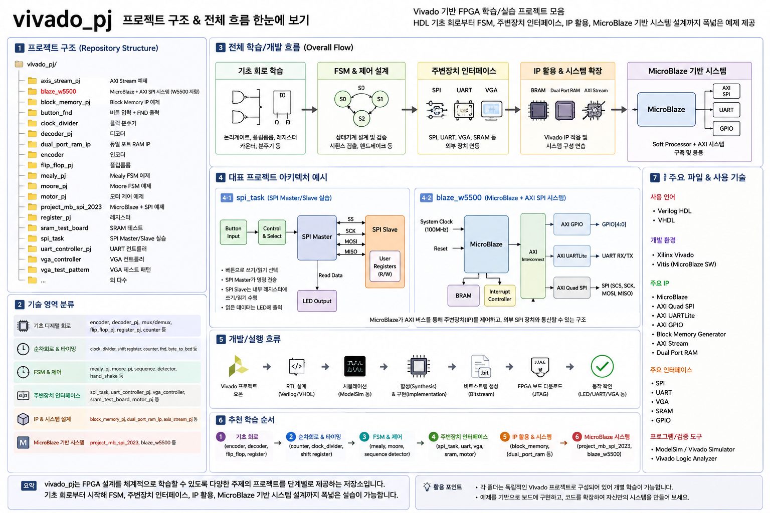
The repository contains many folders that reflect a step-by-step FPGA learning path: basic logic blocks, registers, counters, clock dividers, FSM examples, SPI, UART, VGA, SRAM-related work, AXI Stream, memory IP, MicroBlaze projects, and a W5500-oriented Vivado design. The repository description is short, “Aiot Vivado 프로젝트,” and the repository language breakdown is dominated by VHDL and Verilog, which matches its FPGA/HDL practice nature.
This makes the repository more valuable as a hands-on FPGA learning archive than as a polished production-ready IP package.
What This Project Is
This project can be summarized as:
A Vivado-based FPGA practice collection that moves from basic HDL circuits to interface controllers and MicroBlaze-based AXI peripheral integration.
The project includes examples for:
| Area | Examples / Meaning |
|---|---|
| Basic digital logic | Encoder, decoder, mux/demux, flip-flop, register, counter |
| Timing and display | Clock divider, 7-segment/FND, BCD conversion |
| FSM design | Mealy/Moore machines, sequence detectors, handshake logic |
| Peripheral interfaces | SPI, UART, VGA, SRAM, motor-related control |
| Vivado IP usage | Block memory, dual-port RAM, custom IP, AXI Stream |
| Soft processor system | MicroBlaze, AXI Quad SPI, UARTLite, GPIO |
| W5500-oriented integration | MicroBlaze + AXI SPI structure targeting an SPI Ethernet controller |
The repository root lists many project folders, including axis_stream_pj, blaze_w5500, block_memory_pj, button_fnd, clock_divider, dual_port_ram_ip, encoder, flip_flop_pj, project_mb_spi_2023, spi_task, uart_controller_pj, and multiple VGA-related projects.
Core Technical Value
The value of this repository is not in polished documentation. It is in the breadth of actual Vivado project material.
The repository shows a natural FPGA learning progression:
Basic HDL logic
→ Sequential logic and clocked design
→ FSM-based control
→ Peripheral protocol handling
→ Vivado IP usage
→ MicroBlaze + AXI-based system construction
→ SPI-based external device integration
This progression is technically meaningful because FPGA learners often struggle to connect small HDL examples to larger system-level designs. This repository gives examples across both ends of that path.
System-Level Structure
At a high level, the repository can be viewed as four layers.
[Layer 1] Basic HDL Blocks
    - Encoder / Decoder
    - Flip-Flop / Register
    - Counter / Clock Divider
    - Mux / Demux

[Layer 2] Control Logic
    - FSM
    - Mealy / Moore
    - Sequence Detector
    - Handshake

[Layer 3] Peripheral Interfaces
    - SPI
    - UART
    - VGA
    - SRAM
    - Motor control examples

[Layer 4] Vivado IP and MicroBlaze Systems
    - Block Memory
    - Dual-Port RAM
    - AXI Stream
    - MicroBlaze
    - AXI Quad SPI
    - AXI UARTLite
    - AXI GPIO
    - W5500-oriented SPI interface
This makes the project useful not just for HDL syntax practice, but also for understanding how FPGA designs become embedded systems.
Key Example 1: SPI Task
One of the clearer examples is the spi_task project. Its source folder includes files such as btn_in.v, clockdivider.v, counter.v, datamux4x1.v, fnddecoder.v, spi_master.v, spi_slave.v, and spi_task.v.
The top-level spi_task module receives reset, clock, four button inputs, and drives an 8-bit LED output.
A simplified structure is:
Button input
→ Button conditioning
→ Write/read command selection
→ SPI master
→ SPI slave
→ Internal user registers
→ LED output
The SPI master module exposes typical SPI transaction signals such as ss, sck, mosi, and miso, along with control/data ports such as start_w, start_r, addr, wdata, rdata, and done.
The SPI master also uses state names such as M_IDLE, M_READY, M_SEND, and M_DONE, making it a useful FSM-based SPI learning example.
The SPI slave side defines user register addresses and stores values into user_reg1 through user_reg4, which makes the example easier to understand as a small register-mapped SPI device.
Interpretation
This SPI example is best seen as an educational SPI master/slave loopback or register-access practice design, not as a production-grade SPI IP core.
Its value is that it exposes:
- SPI signal flow
- FSM-based transaction sequencing
- Register read/write modeling
- Button-driven test input
- LED-based visible output
Its limitation is that it is written more like a learning project than a reusable industrial IP block. That is not a sin. It is just what it is, which is apparently a rare concept in technical marketing.
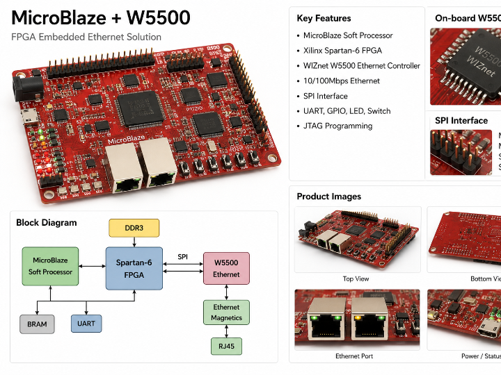
Key Example 2: MicroBlaze and W5500-Oriented Design
The repository includes a blaze_w5500 Vivado project folder. This folder contains Vivado-generated project structures such as .cache, .gen, .hw, .ip_user_files, .runs, .srcs, and .xpr.
The top module blaze_W5500Top.v exposes:
reset
sys_clock
uart_rxd
uart_txd
gpio_out[4:0]
spi_scs
spi_sck
spi_mosi
spi_miso
It instantiates a Vivado block design named system and connects UART, GPIO, and SPI signals to external ports.
The system.bd file shows that the block design includes microblaze_0 using xilinx.com:ip:microblaze:11.0. The design also has a 100 MHz system clock input.
The same block design includes axi_quad_spi_0 using xilinx.com:ip:axi_quad_spi:3.2, with FIFO depth set to 256 and SPI mode set to 0. It also includes axi_uartlite_0 with a 115200 baud rate configuration.
AMD describes MicroBlaze as a 32-bit and 64-bit soft processor included in the Vivado Design Suite, and AMD’s AXI Quad SPI IP connects an AXI4 interface to SPI slave devices supporting standard, dual, or quad SPI protocols.
Simplified Architecture
External Clock / Reset
        ↓
Vivado Block Design: system
        ↓
MicroBlaze Soft Processor
        ↓
AXI Interconnect
   ┌────┼─────────────┐
   ↓    ↓             ↓
AXI GPIO  AXI UARTLite  AXI Quad SPI
   ↓        ↓             ↓
GPIO      UART          SPI pins
                         ↓
                  W5500-oriented interface
W5500 / TOE Interpretation
The folder name blaze_w5500 and the exposed SPI signals suggest that this design is intended to connect a MicroBlaze-based FPGA system to a W5500-like SPI Ethernet controller.
The W5500 itself is a hardwired TCP/IP Ethernet controller that provides Ethernet connectivity through SPI and integrates TCP/IP, 10/100 Ethernet MAC, and PHY functions. WIZnet describes it as supporting protocols such as TCP, UDP, IPv4, ICMP, ARP, IGMP, and PPPoE, with SPI support up to 80 MHz and internal socket buffers.
However, based on the repository evidence checked here, the confirmed part is the hardware-side MicroBlaze + AXI Quad SPI + external SPI pin structure. Full W5500 software initialization, socket control, TCP/UDP communication, or complete TOE usage is not clearly confirmed from the inspected files.
TOE Judgment
| Item | Judgment |
|---|---|
| W5500-oriented project folder exists | Confirmed |
| SPI pins exposed for an external SPI device | Confirmed |
| MicroBlaze + AXI Quad SPI structure exists | Confirmed |
| W5500 register/socket driver code confirmed | Not clearly confirmed |
| Actual TCP/UDP communication confirmed | Not clearly confirmed |
| TOE usage confirmed at application level | Not confirmed |
So the safest conclusion is:
The repository contains a W5500-oriented MicroBlaze/SPI hardware integration structure, but it should not be described as a fully verified W5500 TCP/IP offload application unless additional software-side evidence is confirmed.
Why This Project Matters
This repository matters because it bridges three learning levels that are often separated:
- HDL fundamentals
- Logic blocks, registers, counters, FSMs
- Peripheral control
- SPI, UART, VGA, SRAM, motor-related control
- Embedded FPGA system design
- MicroBlaze, AXI, Vivado IP, SPI-based external device integration
For learners, this is useful because FPGA development is not just “writing Verilog.” Real FPGA systems require timing, interfaces, IP integration, constraints, peripheral communication, and debugging.
This repository gives practical material across those areas, even though it does not package them into a polished tutorial.
Strengths
| Strength | Explanation |
|---|---|
| Wide learning coverage | Covers basic HDL, FSMs, interfaces, IP, and MicroBlaze |
| Real Vivado project structure | Includes actual Vivado project folders, not only isolated code snippets |
| Useful SPI example | spi_task shows master/slave flow and register-style access |
| MicroBlaze system example | blaze_w5500 shows a soft-processor-based AXI peripheral structure |
| Good FPGA learning path | Moves naturally from small logic blocks to system-level integration |
Limitations
| Limitation | Explanation |
|---|---|
| Sparse documentation | The repository has little explanatory README-style guidance |
| Heavy project files | Vivado-generated files are included, which may make the repository bulky |
| Unclear license | Reuse conditions are not obvious from the inspected repository page |
| Not production-ready | The examples appear educational and should be reviewed before reuse |
| W5500 operation not fully proven | Hardware structure exists, but complete W5500 TCP/IP behavior is not clearly shown |
Recommended Audience
This repository is most suitable for:
- FPGA/Vivado beginners
- HDL learners using VHDL or Verilog
- Embedded developers moving toward FPGA
- Students practicing SPI, UART, VGA, FSM, and memory IP
- Developers studying MicroBlaze and AXI peripheral integration
- Engineers exploring how W5500-like SPI Ethernet controllers may be attached to FPGA systems
It is less suitable for:
- Developers looking for polished documentation
- Teams looking for production-certified FPGA IP
- Projects requiring a clearly licensed reusable codebase
- Users expecting a complete W5500 TCP/IP application stack
Suggested Learning Path
A practical way to study this repository would be:
1. Basic logic
   - encoder
   - decoder_pj
   - mux/demux
   - flip_flop_pj

2. Sequential logic
   - register projects
   - shift register projects
   - counter
   - clock_divider

3. FSM control
   - mealy/moore examples
   - sequence detector examples
   - hand_shake

4. Peripheral interfaces
   - spi_task
   - uart_controller_pj
   - vga_controller projects
   - sram_test_board

5. Vivado IP and processor system
   - block_memory_pj
   - dual_port_ram_ip
   - axis_stream_pj
   - project_mb_spi_2023
   - blaze_w5500
This sequence is more useful than opening folders alphabetically, because alphabetical learning is how people accidentally turn education into filing cabinet archaeology.
Final Technical Assessment
vivado_pj is a broad Vivado FPGA practice repository. Its strongest value is educational: it shows how a learner can move from basic HDL blocks to FSMs, peripheral interfaces, Vivado IP, and MicroBlaze-based embedded FPGA systems.
The spi_task project is useful for understanding SPI transaction flow through a master/slave register-access model. The blaze_w5500 project is useful for studying how MicroBlaze, AXI Quad SPI, UARTLite, GPIO, and external SPI pins can be combined into a system that could target a W5500-style SPI Ethernet controller.
However, the repository should not be presented as a finished W5500 networking solution unless the software-side TCP/IP or socket-control implementation is separately verified. Its correct positioning is:
A practical FPGA/Vivado learning repository with useful examples for HDL, peripheral control, MicroBlaze, AXI, and W5500-oriented SPI integration.
Vivado 기반 FPGA 실습 프로젝트와 SPI/UART/VGA, MicroBlaze, W5500 지향 통합 구조
1. 프로젝트 개요
vivado_pj는 AMD/Xilinx Vivado 환경에서 FPGA 설계를 실습하기 위한 프로젝트 모음이다. 단일 완성 제품이라기보다는, 여러 개의 Vivado 실습 프로젝트를 한 저장소에 누적해 둔 FPGA 학습용 프로젝트 아카이브에 가깝다.
저장소에는 기본 논리회로, 레지스터, 카운터, 클럭 분주기, FSM, SPI, UART, VGA, SRAM, AXI Stream, 메모리 IP, MicroBlaze, W5500 지향 설계까지 다양한 예제가 포함되어 있다. 저장소 설명은 “Aiot Vivado 프로젝트”로 표시되어 있으며, 언어 비중은 VHDL과 Verilog가 대부분을 차지한다.
따라서 이 프로젝트는 “완성형 제품 코드”라기보다, FPGA 설계 학습자가 단계적으로 구조를 익히기 위한 실습 묶음으로 보는 것이 정확하다.
2. 이 프로젝트의 핵심 정의
이 프로젝트는 다음과 같이 정의할 수 있다.
Vivado 기반 FPGA 실습 저장소로, HDL 기초 회로에서 시작해 FSM, 주변장치 제어, Vivado IP, MicroBlaze 기반 AXI 시스템, W5500 지향 SPI 연결 구조까지 확장되는 학습 프로젝트 모음이다.
저장소 루트에는 axis_stream_pj, blaze_w5500, block_memory_pj, button_fnd, clock_divider, dual_port_ram_ip, encoder, flip_flop_pj, project_mb_spi_2023, spi_task, uart_controller_pj, 여러 VGA 관련 프로젝트 등이 포함되어 있다.
3. 전체 구조 해석
이 저장소의 전체 흐름은 다음 네 단계로 정리할 수 있다.
1단계: HDL 기본 회로
    - Encoder / Decoder
    - Mux / Demux
    - Flip-Flop
    - Register
    - Counter
    - Clock Divider

2단계: FSM 기반 제어
    - Mealy / Moore FSM
    - Sequence Detector
    - Handshake
    - Button Control

3단계: 주변장치 인터페이스
    - SPI
    - UART
    - VGA
    - SRAM
    - Motor Control

4단계: Vivado IP / MicroBlaze 시스템
    - Block Memory
    - Dual-Port RAM
    - AXI Stream
    - MicroBlaze
    - AXI Quad SPI
    - AXI UARTLite
    - AXI GPIO
    - W5500 지향 SPI 연결
즉, 이 저장소는 FPGA를 처음 배우는 사람이 단순 회로부터 시작해 주변장치, IP, Soft Processor 시스템으로 올라가는 흐름을 보여준다.
이 점이 중요하다. FPGA 학습에서 가장 흔한 문제는 “AND 게이트는 알겠는데 그래서 시스템은 어떻게 만드냐”는 벽이다. 이 저장소는 그 벽을 건너가는 중간 예제들을 꽤 많이 가지고 있다.
4. 주요 기술 영역
4.1 기본 디지털 회로
저장소에는 encoder, decoder_pj, mux/demux, flip_flop_pj, register, shift, counter, clock_divider 계열 프로젝트가 포함되어 있다.
이 영역은 FPGA 학습의 가장 기본이 되는 부분이다.
| 구성 | 의미 |
|---|---|
| Encoder / Decoder | 입력 신호와 코드 변환 |
| Mux / Demux | 여러 신호 중 선택 또는 분배 |
| Flip-Flop | 클럭 기반 1비트 상태 저장 |
| Register | 여러 비트 상태 저장 |
| Counter | 이벤트나 클럭 수 카운트 |
| Clock Divider | 입력 클럭을 낮은 주파수로 분주 |
| FND / 7-Segment | 숫자 표시 출력 제어 |
이 단계는 FPGA가 소프트웨어처럼 한 줄씩 실행되는 구조가 아니라, 하드웨어 회로가 병렬로 구성되는 구조라는 점을 익히는 데 중요하다.
4.2 FSM 기반 제어
저장소에는 Mealy/Moore FSM, sequence detector, handshake 관련 프로젝트가 포함되어 있다.
FSM은 FPGA 설계에서 거의 필수적인 사고방식이다. SPI 송수신, UART 제어, VGA 타이밍, 메모리 제어, 버튼 입력 처리 등은 대부분 상태 기반으로 설계된다.
일반적인 FSM 흐름은 다음과 같다.
입력 감지
→ 현재 상태 확인
→ 조건 판단
→ 다음 상태 결정
→ 출력 제어
→ 다음 클럭에서 상태 갱신
이 저장소가 단순 회로 예제에서 주변장치 제어로 확장될 수 있는 이유도 FSM 예제들이 중간에 있기 때문이다.
4.3 주변장치 인터페이스
이 저장소에는 SPI, UART, VGA, SRAM, Motor 관련 프로젝트들이 포함되어 있다.
| 인터페이스 | 학습 의미 |
|---|---|
| SPI | 동기식 직렬 통신, Master/Slave 구조 |
| UART | 비동기 직렬 통신 |
| VGA | 픽셀 클럭, 수평/수직 동기, 영상 타이밍 |
| SRAM | 외부 메모리 접근 |
| Motor | 외부 구동 장치 제어 |
| Button/FND | 사람 입력과 표시 출력 연결 |
이 영역은 FPGA 학습이 “문법 연습”에서 “실제 하드웨어 제어”로 넘어가는 구간이다.
5. 핵심 예제 1: spi_task
spi_task는 이 저장소에서 구조를 설명하기 좋은 예제다. 해당 소스 폴더에는 btn_in.v, clockdivider.v, counter.v, datamux4x1.v, fnddecoder.v, spi_master.v, spi_slave.v, spi_task.v, top_fndcontrol.v 등이 포함되어 있다.
spi_task.v의 top module은 reset, clock, 4비트 버튼 입력, 8비트 LED 출력을 가진다.
구조를 단순화하면 다음과 같다.
Button Input
    ↓
Button Debounce / Selection
    ↓
Write Data / Read Address Selection
    ↓
SPI Master
    ↓  ss / sck / mosi / miso
SPI Slave
    ↓
Internal User Registers
    ↓
Read Data
    ↓
LED Output
5.1 SPI Master
spi_master.v는 reset, clock, freq, start_w, start_r, addr, wdata, rdata, done, ss, sck, mosi, miso 같은 포트를 가진다. 즉, SPI 트랜잭션을 제어하고 외부 SPI 신호를 생성하는 모듈이다.
이 SPI Master는 M_IDLE, M_READY, M_SEND, M_DONE 상태를 사용한다.
M_IDLE
→ M_READY
→ M_SEND
→ M_DONE
→ M_IDLE
이는 SPI 전송을 FSM으로 다루는 전형적인 학습 구조다.
5.2 SPI Slave
spi_slave.v는 rUSER_REG1, rUSER_REG2, rUSER_REG3, rUSER_REG4 같은 사용자 레지스터 주소를 정의하고, 내부에 user_reg1부터 user_reg4까지의 레지스터를 갖는다.
이 구조는 SPI Slave를 단순한 신호 수신기가 아니라, 주소 기반으로 내부 레지스터에 접근하는 작은 주변장치처럼 모델링한다.
5.3 의미
spi_task는 다음을 학습하기 좋다.
- SPI Master 동작
- SPI Slave 동작
- SPI 신호 흐름
- FSM 기반 전송 제어
- 주소/데이터 기반 레지스터 접근
- 버튼 입력을 통한 실험
- LED 출력으로 결과 확인
다만 이 코드는 제품용 SPI IP라기보다 교육용 실습 코드에 가깝다. 코드 스타일, 검증, 예외 처리, 타이밍 안정성은 실제 사용 전에 별도 검토가 필요하다. 인간도 실습과 제품을 구분해야 하는데, 이 단순한 일을 업계 전체가 종종 실패합니다.
6. 핵심 예제 2: blaze_w5500
blaze_w5500 폴더는 Vivado 프로젝트 형태를 유지하고 있으며, .cache, .gen, .hw, .ip_user_files, .runs, .srcs, .xpr 같은 Vivado 생성물과 프로젝트 파일을 포함한다.
이 프로젝트의 top module인 blaze_W5500Top.v는 다음 외부 포트를 가진다.
reset
sys_clock
uart_rxd
uart_txd
gpio_out[4:0]
spi_scs
spi_sck
spi_mosi
spi_miso
내부에서는 system이라는 Vivado Block Design을 인스턴스화하고, reset, clock, UART, GPIO, SPI 신호를 연결한다.
7. MicroBlaze / AXI 구조
system.bd에는 microblaze_0가 포함되어 있으며, 해당 IP는 xilinx.com:ip:microblaze:11.0으로 표시된다. 또한 시스템 클럭 입력은 100 MHz로 설정되어 있다.
같은 Block Design 안에는 axi_quad_spi_0도 포함되어 있으며, 이는 xilinx.com:ip:axi_quad_spi:3.2로 표시된다. FIFO depth는 256, SPI mode는 0으로 설정되어 있다. axi_uartlite_0도 포함되어 있으며 baud rate는 115200으로 설정되어 있다.
AMD 공식 문서 기준 MicroBlaze는 Vivado Design Suite에 포함되는 32-bit 및 64-bit soft processor이고, AXI Quad SPI는 AXI4 인터페이스를 Standard/Dual/Quad SPI 장치와 연결하는 IP다.
구조를 정리하면 다음과 같다.
External Clock / Reset
        ↓
Vivado Block Design: system
        ↓
MicroBlaze Soft Processor
        ↓
AXI Interconnect
   ┌────┼─────────────┐
   ↓    ↓             ↓
AXI GPIO  AXI UARTLite  AXI Quad SPI
   ↓        ↓             ↓
GPIO      UART          SPI
                         ↓
                  W5500 지향 외부 연결
8. W5500 / TOE 적용 여부
8.1 확인된 것
이 저장소에서 확인되는 것은 다음이다.
| 항목 | 확인 여부 |
|---|---|
blaze_w5500 프로젝트 폴더 | 확인 |
| SPI 외부 포트 노출 | 확인 |
| MicroBlaze 포함 | 확인 |
| AXI Quad SPI 포함 | 확인 |
| UARTLite / GPIO 포함 | 확인 |
| W5500 레지스터 제어 코드 | 명확한 확인 부족 |
| TCP/UDP 소켓 동작 코드 | 명확한 확인 부족 |
8.2 W5500의 일반적 역할
W5500은 SPI를 통해 임베디드 시스템에 Ethernet 연결을 제공하는 Hardwired TCP/IP Ethernet Controller다. WIZnet 공식 설명에 따르면 W5500은 TCP/IP stack, 10/100 Ethernet MAC, PHY를 내장하고, TCP, UDP, IPv4, ICMP, ARP, IGMP, PPPoE 등을 지원한다. 또한 SPI는 최대 80 MHz까지 지원한다고 설명된다.
즉, W5500 자체는 다음 역할을 한다.
MCU / FPGA / Processor
    ↓ SPI
W5500
    ↓ Hardwired TCP/IP + MAC + PHY
Ethernet Network
8.3 이 저장소에서의 판정
blaze_w5500이라는 폴더명과 MicroBlaze + AXI Quad SPI + 외부 SPI 핀 구조를 보면, 이 프로젝트는 W5500 같은 SPI 기반 Ethernet 컨트롤러를 FPGA 시스템에 연결하려는 구조로 해석할 수 있다.
하지만 현재 확인된 범위에서는 W5500 초기화, 레지스터 접근, socket open/close, TCP/UDP 송수신 코드가 명확히 확인되지 않는다.
따라서 최종 판정은 다음과 같다.
이 저장소는 W5500 지향 MicroBlaze/SPI 하드웨어 구조를 포함하지만, W5500의 TCP/IP Offload 기능을 실제 애플리케이션 수준에서 사용한다고 단정하기는 어렵다.
TOE 관점으로 더 냉정하게 말하면:
| 항목 | 판정 |
|---|---|
| W5500 자체가 TOE 성격의 칩인가 | 그렇다 |
| 이 프로젝트가 W5500 연결을 의도한 구조인가 | 가능성이 높다 |
| 이 프로젝트에서 TOE 기능 사용이 검증되었는가 | 확인 부족 |
| “TOE 적용 완료 프로젝트”라고 표현 가능한가 | 부적절 |
| “W5500 지향 SPI/MicroBlaze 통합 구조”라고 표현 가능한가 | 적절 |
9. 기술적 장점
9.1 학습 범위가 넓다
기초 HDL부터 MicroBlaze 기반 시스템까지 포함되어 있다. FPGA를 처음 배우는 입장에서는 단편 예제 여러 개를 찾는 것보다 이런 누적 저장소가 더 실용적일 수 있다.
9.2 실제 Vivado 프로젝트 구조가 남아 있다
Vivado 프로젝트 생성물까지 포함되어 있어, 단순 코드 조각만 보는 것보다 프로젝트 구조를 파악하기 쉽다. 물론 Git 저장소 관점에서는 무거워질 수 있다. 개발자들은 항상 “재현성”과 “저장소 청결성” 사이에서 고통받는데, 컴퓨터는 아무 잘못이 없습니다.
9.3 SPI Master/Slave 실습이 구체적이다
spi_task는 버튼 입력에서 SPI Master/Slave, 내부 레지스터, LED 출력까지 이어지는 구조라서 SPI 통신 흐름을 눈으로 따라가기 좋다.
9.4 MicroBlaze 기반 시스템 확장 예제가 있다
blaze_w5500은 MicroBlaze, AXI Quad SPI, UARTLite, GPIO를 포함하는 Block Design 기반 프로젝트다. 순수 RTL 실습에서 Soft Processor 기반 FPGA 시스템으로 넘어가는 데 참고할 수 있다.
10. 한계와 주의점
10.1 문서화가 부족하다
저장소 설명은 매우 짧고, 각 프로젝트의 목적, 보드 환경, 빌드 순서, 검증 방법을 설명하는 문서가 부족하다. 처음 보는 사람은 폴더명과 소스 구조를 직접 해석해야 한다.
10.2 Vivado 생성물이 많이 포함되어 있다
.cache, .gen, .hw, .ip_user_files, .runs 같은 Vivado 생성물이 포함되어 있다. 학습용으로는 재현에 도움이 될 수 있지만, 협업용 저장소라면 관리가 부담스러울 수 있다.
10.3 라이선스가 명확하지 않다
확인한 저장소 페이지 기준으로 명확한 라이선스 정보가 보이지 않는다. 따라서 상업적 재사용, 사내 코드 반영, 공개 프로젝트 재배포에는 주의가 필요하다.
10.4 제품용 코드로 바로 쓰기 어렵다
이 저장소의 예제들은 학습과 실습 성격이 강하다. 실제 제품에 적용하려면 다음 검토가 필요하다.
- 타이밍 제약 검토
- 합성 결과 확인
- 보드별 XDC 검증
- CDC 문제 확인
- Reset polarity 정리
- Testbench 보강
- 코드 스타일 정리
- 예외 상황 처리
- 라이선스 확인
11. 이 프로젝트가 적합한 사람
| 대상 | 적합도 | 이유 |
|---|---|---|
| FPGA/Vivado 입문자 | 높음 | 기초 회로부터 주변장치까지 폭넓게 포함 |
| HDL 학습자 | 높음 | VHDL/Verilog 실습 재료가 많음 |
| 임베디드 개발자 | 높음 | SPI/UART/W5500 관점에서 FPGA 구조를 볼 수 있음 |
| MicroBlaze 입문자 | 중간~높음 | AXI SPI/UART/GPIO 구조 참고 가능 |
| W5500 FPGA 연결 실험자 | 중간 | 하드웨어 구조 참고 가능, 소프트웨어 검증은 별도 필요 |
| 제품용 IP를 찾는 개발자 | 낮음 | 문서화, 검증, 라이선스 부족 |
12. 추천 학습 순서
이 저장소를 볼 때는 알파벳 순서가 아니라 난이도 순서로 접근하는 편이 낫다.
1. 기본 논리
   - encoder
   - decoder_pj
   - mux/demux
   - flip_flop_pj

2. 순차 회로
   - register 계열
   - shift register 계열
   - counter
   - clock_divider

3. 표시와 입력
   - button_fnd
   - byte_to_bcd
   - fnd / 7-segment 관련 예제

4. FSM
   - mealy_pj
   - moore_pj
   - sequence detector
   - hand_shake

5. 주변장치
   - spi_task
   - uart_controller_pj
   - vga_controller 계열
   - sram_test_board
   - motor_pj

6. IP / Processor
   - block_memory_pj
   - dual_port_ram_ip
   - axis_stream_pj
   - project_mb_spi_2023
   - blaze_w5500
13. 저자 정보
GitHub 프로필 기준 작성자는 MongRaGong / a06729로 표시된다. 공개 프로필에는 저장소 39개, Stars 204개, Followers 2명, Following 0명이 표시되어 있다.
현재 확인 가능한 공개 정보만 기준으로 하면, 작성자는 Vivado/FPGA 실습뿐 아니라 여러 개발 실습 저장소를 관리하는 GitHub 사용자로 볼 수 있다. 다만 실명, 소속, 직무 이력은 이 저장소와 공개 프로필 범위에서 명확히 확인되지 않으므로 단정하지 않는 것이 맞다.
-
vivado_pj
