



Hardware TCP/IP Stack in a Network Encryption Card
A Chinese supercomputing institute's network data encryption card routes its protocol communication through the W5500's hardwired TCP/IP stack.
How to Build a Hardware TCP/IP Network Encryption Card with W5500 on STM32F732RET6?
Summary
CN116707970A describes a network data encryption card built around an STM32F732RET6-based cryptographic processing stage and two WIZnet W5500 Ethernet controllers per card. One W5500 receives network traffic, the cryptographic module encrypts or decrypts the payload, and the second W5500 returns the processed data to Ethernet. The W5500 provides the hardware TCP/IP transport layer, allowing the STM32-based security subsystem to concentrate on cryptographic processing rather than implementing the TCP/IP stack in software.
What the Project Does
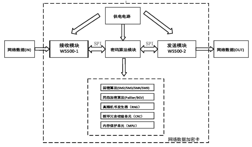
The patent proposes an inline network-security architecture in which both communicating endpoints connect through dedicated network data encryption cards. At the sending side, data enters the card through a receive module, passes through a cryptographic algorithm module, and leaves through a transmit module. A corresponding card at the receiving side reverses the process and delivers the recovered plaintext to the destination.
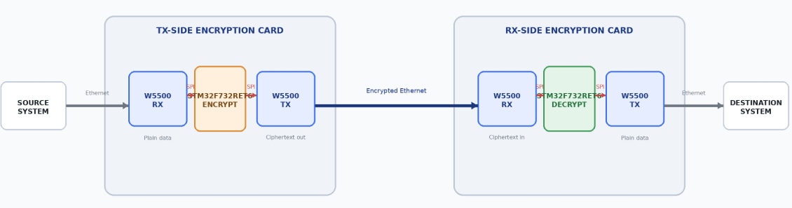
The design separates the system into three main processing blocks:
Ethernet receive → cryptographic processing → Ethernet transmit
The patent identifies W5500 devices for both Ethernet blocks. The cryptographic subsystem supports SM2, SM3, SM4, and SM9 algorithms and describes SM4 ECB, CBC, OFB, CFB, and CTR modes. It also specifies Paillier, BGV, and CKKS homomorphic-encryption functions, along with a true-random-number generator, memory protection, and CRC processing.
For the central processing stage, the document identifies an STM32F732RET6, a Cortex-M7 MCU operating at up to 216 MHz, and describes an ED-ML-01 encryption module. The patent lists 512 KB of Flash and 256 KB of SRAM for the STM32-based processing subsystem.
The important data path is therefore:
Endpoint → W5500 RX → SPI → cryptographic module → SPI → W5500 TX → Ethernet channel
At the remote card, the same structure receives the ciphertext, decrypts it, and returns the original data to the destination.
Where WIZnet Fits
The WIZnet component is explicitly identified as the W5500. This is not an inferred replacement or suggested upgrade: W5500 is part of the patent claims themselves. Claim 7 states that the hardware protocol communication is implemented using a W5500 with an integrated TCP/IP protocol stack, while Claim 8 states that the cryptographic module controls W5500 initialization and reset.
Each encryption card contains two distinct W5500 functions:
W5500-1 — receive side: terminates the incoming Ethernet/TCP/IP connection and makes received data available to the cryptographic processor through SPI.
W5500-2 — transmit side: accepts the processed data from the cryptographic processor through SPI and transmits it to the next Ethernet endpoint.
This separation is visible in the patent architecture, where both W5500 devices connect independently to the cryptographic algorithm module over SPI.
The W5500 is therefore not the encryption engine. Its job is Ethernet and TCP/IP transport. Encryption, key handling, authentication, homomorphic processing, and CRC-related operations belong to the security subsystem.
That division of responsibilities is technically significant because cryptographic workloads already consume MCU processing and memory resources. The patent specifically contrasts its architecture with software protocol implementations that require developers to implement and maintain networking layers on the host processor.
WIZnet specifies that the W5500 contains a hardwired TCP/IP stack, integrated 10/100 Ethernet MAC and PHY, eight independent hardware sockets, 32 KB of internal TX/RX memory, and an SPI interface operating at up to 80 MHz. Those are device capabilities; the patent does not specify its actual SPI clock, socket-buffer allocation, or measured network throughput. (WIZnet 문서 시스템)
This makes the architectural split straightforward:
STM32/security module
encryption and decryption
key/security operations
data inspection and transformation
W5500 control
W5500
Ethernet MAC/PHY
IPv4/TCP/UDP processing
socket buffering
network transmit and receive
Implementation Notes
The patent provides circuit diagrams and architectural descriptions but does not provide firmware source code. Consequently, there is no repository implementation from which initialization or socket code can be reproduced.
Two translated excerpts establish how W5500 is actually used.
CN116707970A.pdf — Claim 7 / paragraph [0057]
“Hardware protocol communication is implemented through the W5500 hardware protocol stack chip with built-in TCP/IP.”
This establishes W5500 as the network protocol engine rather than merely an external PHY.
CN116707970A.pdf — paragraph [0075]
“The cryptographic algorithm module sends commands to initialize and reset W5500.”
The same paragraph explains that received data is read from the receive-side W5500 over SPI, encrypted, and then written through SPI to the transmit-side W5500.
The resulting transmit sequence is:
1. Receive network data.
The ingress W5500 receives data originating from the sending endpoint.
2. Transfer it over SPI.
The cryptographic processing module reads the received data from the ingress W5500.
3. Perform security processing.
The cryptographic module applies the required encryption operation.
4. Transfer ciphertext to the second W5500.
The encrypted result is written over SPI to the egress W5500.
5. Transmit through Ethernet.
The egress W5500 sends the ciphertext toward the remote encryption card.
For receive-side recovery, the process is reversed: ciphertext enters through W5500, the cryptographic module decrypts it, and the resulting plaintext passes to the second W5500 for delivery to the receiving endpoint.
The circuit drawings additionally show independent receive and transmit W5500 sections, Ethernet ports, clock circuitry, and separate connections toward the security-processing block. The power circuit derives 3.3 V supplies from a 5 V input and distinguishes digital and analog supply domains in the illustrated implementation.
Practical Tips / Pitfalls
Treat the two W5500 devices as independent network interfaces. Maintain separate chip-select, reset, interrupt, socket, and network-state handling for ingress and egress rather than assuming they share protocol state.
Budget SPI bandwidth together with cryptographic throughput. A 100 Mbps Ethernet PHY does not imply 100 Mbps encrypted application throughput. Traffic must cross W5500-to-MCU SPI, pass through encryption, and then cross another SPI connection. W5500 itself supports SPI clocks up to 80 MHz, but the patent provides no end-to-end throughput measurement. (WIZnet 문서 시스템)
Define IP configuration explicitly for both sides. The patent does not specify DHCP, static addressing, socket numbers, or connection-management policy. These must be defined in production firmware for each W5500 independently.
Plan socket and buffer allocation around expected sessions. W5500 supplies eight hardware sockets and 32 KB of internal TX/RX memory. Allocate those resources according to the number and size of simultaneous encrypted flows rather than relying automatically on an example configuration. (WIZnet 문서 시스템)
Provide recovery for link and SPI faults. The patent explicitly places W5500 initialization and reset under control of the cryptographic module. Firmware should also monitor link state, stalled sockets, SPI failures, and encryption-processing timeouts before deciding whether to reset a network interface.
Account for backpressure between networking and encryption. If cryptographic processing is slower than incoming network traffic, buffering can fill before the security engine drains it. The patent describes the processing sequence but does not define a queueing or flow-control strategy.
Treat Ethernet layout and power integrity as part of the security appliance design. Follow W5500 PHY routing, magnetics, grounding, decoupling, and EMI practices carefully, particularly when receive and transmit Ethernet interfaces operate simultaneously on the same board.
FAQ
Q: Why does this network encryption card use W5500?
The patent uses W5500 to move TCP/IP processing away from the cryptographic processor. Its stated objective is to avoid the complexity and resource consumption associated with implementing network protocol layers in software while leaving the STM32-based subsystem available for encryption and security processing. W5500 provides the hardwired TCP/IP stack, Ethernet MAC/PHY, socket engine, and packet buffers required for that separation.
Q: How does W5500 connect to the STM32-based encryption platform?
The patent connects the receive and transmit modules to the cryptographic algorithm module through SPI. The controller initializes and resets the W5500 devices and transfers payload data through those SPI connections. The document does not disclose the configured SPI frequency or complete firmware-level pin assignment.
Q: What exactly does W5500 do in this encryption-card design?
One W5500 receives the original network stream and supplies its payload to the encryption subsystem. A second W5500 takes the resulting ciphertext and transmits it over Ethernet. On the remote card, the corresponding receive W5500 accepts ciphertext and the second interface delivers decrypted data to the destination. W5500 handles networking; it does not perform SM2, SM3, SM4, SM9, or homomorphic encryption.
Q: Can a beginner build this W5500 encryption card from the patent?
It is better suited to an intermediate or advanced embedded developer. Basic W5500 socket operation is comparatively straightforward, but reproducing the complete design requires SPI firmware, dual Ethernet interfaces, STM32 development, Ethernet PCB layout, network-session management, buffering, and correct cryptographic/key-management implementation. The patent provides schematics and architecture but not complete production firmware.
Q: How does the W5500 approach compare with an MCU running LwIP?
W5500 implements TCP/UDP/IPv4 and related protocols in dedicated hardware and provides its own socket buffers, reducing the networking code, RAM usage, and protocol-processing workload placed on the cryptographic MCU. An LwIP-based design processes the TCP/IP stack on the MCU, giving developers more software-level flexibility and capabilities such as IPv6 depending on configuration, but consuming host CPU and memory resources. The patent itself contrasts W5500 with software protocol-stack processing, although it does not specifically name or benchmark LwIP.
Source
Original patent: CN116707970A, Network Data Encryption Card Based on Hardware Protocol and Transmission Method, filed July 4, 2023 and published September 5, 2023. The applicant is Jinan Supercomputing Technology Research Institute.
Original patent PDF — CN116707970A
W5500 technical reference: WIZnet product documentation for the hardwired TCP/IP stack, SPI interface, sockets, and internal buffer architecture. (WIZnet 문서 시스템)
License: No open-source or content reuse license is stated in the patent publication; it is a published patent application rather than an open-source software project.
Tags
#W5500 #STM32F732RET6 #Ethernet #HardwareTCPIP #NetworkSecurity #SPI #SM4 #SM2 #HomomorphicEncryption #IndustrialIoT