



How to Wire W5500 to STM32F103 for an Industrial IoT Ethernet Node?
This repository provides a schematic PDF for connecting an STM32F103 microcontroller to a WIZnet W5500 Ethernet controller.
How to Wire W5500 to STM32F103 for an Industrial IoT Ethernet Node?
Summary
This repository provides a schematic PDF for connecting an STM32F103 microcontroller to a WIZnet W5500 Ethernet controller. In an Industrial IoT design, the STM32F103 supplies application control and communicates with the W5500 through SPI, while the W5500 provides the Ethernet MAC, PHY, hardwired TCP/IP engine, socket state, and packet buffering. The repository is useful as a circuit reference, but its schematic should be checked against current WIZnet reference designs before being used in production.
What the Project Does
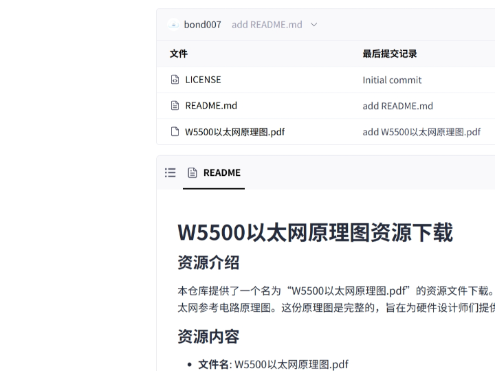
The repository contains a README, an MIT license, and a file named W5500以太网原理图.pdf. Its description identifies the document as a complete W5500 Ethernet reference schematic using an STM32F103 as the main controller. The stated audience includes hardware designers, embedded developers, students, and electronics enthusiasts.
The repository is a hardware-documentation resource rather than a firmware application. It does not provide visible source code for SPI initialization, socket control, DHCP, TCP, UDP, or application protocols. The GitCode preview confirms that the PDF exists, but the public interface reviewed here does not expose the schematic pages in a form that allows individual component references, resistor values, pin assignments, or net names to be verified.
A production system based on this architecture would use the following signal and data paths:
Industrial sensors or control interfaces → STM32F103 application firmware → SPI → W5500 → Ethernet magnetics → RJ45 connector → industrial network
The return path carries commands or configuration data from the Ethernet network through the W5500 to the STM32F103 application.
The STM32F103 is expected to manage:
Sensor acquisition and control logic
SPI transactions with the W5500
Network configuration
Socket commands
Application protocols
Fault detection and recovery
The W5500 is expected to manage:
Ethernet MAC and PHY operation
Supported IPv4 and transport protocols
Eight hardware socket contexts
Internal transmit and receive buffering
Link status and socket events
Where WIZnet Fits
The relevant product is the WIZnet W5500. It is a hardwired TCP/IP Ethernet controller that integrates a 10/100 Ethernet MAC, PHY, eight hardware sockets, and 32 KB of internal packet memory. The STM32F103 accesses the device through SPI rather than through a parallel Ethernet MAC interface.
In this Industrial IoT architecture, the W5500 sits between the MCU application and the physical Ethernet network:
STM32F103 GPIO/SPI → W5500 digital interface → W5500 analog Ethernet interface → isolation magnetics → RJ45
This arrangement is useful when the MCU must continue handling sensing, control, field interfaces, alarms, or local user interaction without also running a complete software TCP/IP stack.
The W5500 does not remove all networking responsibilities from the STM32F103. Firmware must still initialize the chip, configure addresses, allocate socket memory, open and recover sockets, implement application-layer protocols, and respond to network failures.
Implementation Notes
The repository confirms that the schematic is intended to show an STM32F103 and W5500 Ethernet circuit, but the public PDF preview does not expose enough detail to quote verified net names, reference designators, or component values. The following sections therefore describe the checks that should be applied when reviewing the downloaded schematic against WIZnet’s official reference design.
STM32F103-to-W5500 SPI Wiring
The minimum SPI interface contains:
STM32 SPI clock to W5500 SCLK
STM32 MOSI to W5500 MOSI
STM32 MISO from W5500 MISO
A dedicated STM32 GPIO to W5500 chip select
A common digital ground
The design should also connect:
An STM32 GPIO to the W5500 reset input
The W5500 interrupt output to an STM32 external-interrupt-capable GPIO when event-driven operation is required
A dedicated GPIO is normally preferable for chip-select control because a complete W5500 transaction includes an address phase, a control phase, and a data phase under one chip-select assertion. The firmware and SPI peripheral configuration must preserve that transaction boundary.
The schematic review should confirm that:
Both devices use compatible 3.3 V logic levels
MISO is not shared with another device that drives the bus while its chip select is inactive
Reset and interrupt signals have defined levels during MCU startup
SPI traces are short and routed over an uninterrupted reference plane
Series damping footprints are available if edge ringing appears during validation
For initial bring-up, the SPI clock should be kept below the target production rate. The clock can be increased after repeated register reads and long burst transfers have been verified.
Power Architecture
The W5500 requires a stable 3.3 V supply for both digital and analog functions. A production schematic should not treat every supply pin as a single undifferentiated connection.
The review should verify:
Local high-frequency decoupling at each W5500 supply group
A nearby bulk capacitor for transient demand
Short return paths from decoupling capacitors to ground
Separation of noisy digital currents from the PHY analog supply path
A regulator with enough startup and transient-current margin
A defined power-up sequence for the STM32F103 and W5500
The W5500 reference circuit also uses an external bias resistor associated with its analog PHY circuitry. The value, tolerance, and placement must follow the official datasheet or reference schematic rather than being selected as a generic pull-down.
For an Industrial IoT board, the 3.3 V rail should be checked under:
Ethernet link establishment
Continuous packet traffic
Cable insertion
MCU peripheral switching
Minimum and maximum input supply
Temperature extremes
Brownout recovery
The regulator should not only meet average current requirements. Its transient response and local decoupling must prevent the W5500 from resetting or corrupting SPI communication during network activity.
Reset Design
The W5500 reset input should be controlled rather than left dependent on an undefined MCU startup state.
A robust design normally includes:
A pull resistor that holds reset in a safe state
An STM32 GPIO for controlled reset
A reset pulse that meets W5500 timing requirements
A delay before register access after reset release
Firmware verification that the device responds correctly before socket initialization
The reset architecture should allow the STM32 to restart the W5500 without resetting the complete controller. This is useful when recovering from a persistent SPI, PHY, or socket fault while preserving industrial process state.
The firmware recovery hierarchy should be:
Close and reopen the failed socket.
Reapply network configuration when necessary.
Reset and reinitialize the W5500.
Reset the complete STM32 system only as a final measure.
The schematic should also prevent the STM32 from unintentionally releasing W5500 reset while the 3.3 V rail is still rising.
Oscillator and Clocking
The W5500 Ethernet block requires a stable reference clock. The downloaded schematic should be checked for:
The specified crystal or oscillator frequency
Correct load capacitors
Short and symmetric crystal traces
Separation from SPI, switching-regulator, and high-current signals
No test pad or long stub that adds excessive capacitance
Ground shielding consistent with the reference layout
A crystal circuit that oscillates on one prototype may still have inadequate startup margin across temperature, component tolerance, and production variation. Clock startup should be included in environmental validation.
Ethernet Magnetics and RJ45 Wiring
The W5500 PHY connects to the cable through isolation magnetics. The magnetics may be implemented as a separate transformer plus RJ45 connector or as an integrated MagJack.
The official WIZnet reference documentation includes different connection recommendations depending on the transformer and center-tap arrangement. It also warns that specific coupling components are required in certain integrated-magnetics configurations and that unsuitable center-tap connections can increase power dissipation.
The schematic review should confirm:
Transformer compatibility with 10/100BASE-T
Correct transmit and receive pair mapping
Correct center-tap treatment
Required termination and coupling components
LED polarity and resistor values
Cable-side ESD protection
Chassis or shield connection strategy
Adequate isolation distance between cable and logic sides
The Ethernet differential pairs should be routed as controlled-impedance pairs with minimal skew, short stubs, and no plane splits beneath them. Magnetics should be placed near the connector so cable-side surge and common-mode currents do not travel through the logic area.
Industrial Protection
A schematic that works on a development bench may require additional protection for an industrial installation.
Depending on the environment, the final board may need:
Ethernet-rated TVS protection
Shield-to-chassis coupling
Common-mode noise control
Reverse-polarity protection
Input surge protection
Filtered or isolated power
Galvanic isolation on external field interfaces
Brownout supervision
Hardware watchdog support
These additions should be selected from the product’s actual EMC, surge, ESD, grounding, and installation requirements. They cannot be validated from the repository description alone.
W5500 Compared with an ENC28J60 Reference Circuit
Both W5500 and ENC28J60 can connect to an STM32F103 over SPI, and both integrate an Ethernet MAC and PHY. Their system responsibilities differ substantially.
The ENC28J60 is a stand-alone 10BASE-T Ethernet controller with an SPI host interface, 8 KB of packet RAM, receive filtering, DMA assistance, and checksum support. Its host controller is responsible for the broader Ethernet and TCP/IP software stack. The Microchip reference architecture also requires a 25 MHz clock, transformer termination components, an external RBIAS resistor, and a capacitor for its internal regulator output.
The W5500 integrates supported TCP/IP processing and eight hardware sockets in addition to its MAC, PHY, and 32 KB packet memory. This changes both the hardware and firmware partition.
W5500 circuit
10/100 Ethernet
SPI-connected host interface
Hardware TCP/IP sockets
32 KB internal packet memory
Application firmware uses socket-oriented control
Lower host-side TCP/IP implementation burden
ENC28J60 circuit
10BASE-T Ethernet
SPI-connected host interface
MAC and PHY without a complete hardware TCP/IP socket engine
8 KB shared packet memory
Host runs the TCP/IP software stack
Greater host-side software and RAM requirements
At the schematic level, both devices require careful 3.3 V power, clocking, SPI wiring, bias components, transformer connections, and ESD protection. The circuit cannot be converted from one controller to the other by replacing only the IC, because pinout, analog requirements, clocking, memory architecture, and firmware model differ.
For an STM32F103 Industrial IoT design, W5500 is generally easier to integrate when predictable MCU memory usage and socket-oriented networking are priorities. ENC28J60 may remain appropriate when 10 Mbps is sufficient and the development team already maintains a proven host-side TCP/IP stack.
Practical Tips / Pitfalls
Do not treat the repository schematic as automatically production-ready. Compare every supply, bias, clock, reset, transformer, and connector connection with the latest WIZnet reference documents.
Give W5500 reset a defined hardware state and an STM32-controlled recovery path. An MCU GPIO that floats during startup can produce intermittent boot failures.
Place decoupling capacitors at the relevant W5500 supply pins, not only near the regulator. Long power traces reduce their effectiveness.
Keep SPI routing separate from crystal and Ethernet analog nodes. Fast SCLK and MOSI edges can disturb marginal PHY or oscillator layouts.
Verify the exact MagJack center-tap arrangement. Integrated connectors with different internal transformer wiring are not always interchangeable.
Include test access for 3.3 V, reset, interrupt, SPI signals, and PHY link state so manufacturing and field failures can be isolated.
Perform cable insertion, ESD, brownout, switch restart, and continuous-traffic tests before freezing the Industrial IoT hardware.
FAQ
Q: Why use the W5500 with STM32F103 in an Industrial IoT controller?
The W5500 combines a 10/100 Ethernet MAC and PHY with hardwired TCP/IP processing, eight sockets, and internal packet memory. This reduces the amount of TCP/IP processing and buffering that must run on the STM32F103, leaving more MCU resources available for sensing, control, diagnostics, and field interfaces.
Q: How does the W5500 connect to the STM32F103?
It connects through SPI using SCLK, MOSI, MISO, and chip select. A practical industrial design should also connect reset and interrupt signals. The exact STM32 pin assignments used in the repository schematic could not be verified from the public PDF preview.
Q: What role does the W5500 play in this schematic?
The W5500 forms the wired network interface. It receives socket commands and payload data from the STM32F103 over SPI, stores packets in internal memory, executes supported TCP/IP operations, and connects to the Ethernet cable through its integrated MAC, PHY, and external isolation magnetics.
Q: Can beginners use this schematic?
A developer with basic STM32, SPI, power-supply, and Ethernet-hardware knowledge can use it as a study reference. Industrial deployment additionally requires understanding of magnetics, differential routing, grounding, ESD, surge protection, EMC testing, reset behavior, and network recovery.
Q: How does the W5500 circuit compare with an ENC28J60 design?
Both use SPI and require an external clock, bias components, isolation magnetics, and careful power design. W5500 adds hardware TCP/IP sockets and 32 KB of packet memory, while ENC28J60 provides a 10 Mbps MAC/PHY and 8 KB packet RAM with the TCP/IP stack primarily running on the MCU. As a result, an ENC28J60 design usually requires more host firmware, RAM, and stack validation.
Source
Original project: Open-source-documentation-tutorial, W5500 Ethernet Schematic Resource Download. The repository contains a README, MIT license, and a PDF described as a complete STM32F103 and W5500 Ethernet reference circuit.
WIZnet technical reference: W5500 product documentation and official reference-schematic guidance, including transformer and integrated-MagJack connection notes.
Comparison reference: Microchip ENC28J60 datasheet and product documentation covering its SPI interface, 10BASE-T MAC/PHY, 8 KB packet memory, clocking, reset, bias, regulator, and transformer requirements.
License: The GitCode repository is marked MIT. The schematic PDF may also contain third-party symbols, manufacturer reference material, or separate notices that should be reviewed before redistribution.
Tags
#W5500 #WIZnet #STM32F103 #IndustrialIoT #EthernetHardware #SPI #PowerDesign #ResetCircuit #MagJack #ENC28J60 #SchematicReview #EmbeddedNetworking
산업용 IoT 이더넷 노드에서 STM32F103과 W5500을 어떻게 연결할 수 있을까?
요약
이 저장소는 STM32F103 마이크로컨트롤러와 WIZnet W5500 이더넷 컨트롤러를 연결하는 회로도 PDF를 제공합니다. 산업용 IoT 설계에서 STM32F103은 애플리케이션 제어를 담당하고 SPI를 통해 W5500과 통신하며, W5500은 이더넷 MAC, PHY, 하드와이어드 TCP/IP 엔진, 소켓 상태, 패킷 버퍼를 제공합니다. 이 저장소는 회로 참고 자료로 활용할 수 있지만, 실제 양산 설계에 적용하기 전에는 최신 WIZnet 공식 레퍼런스 회로와 비교 검토해야 합니다.
프로젝트가 하는 일
저장소에는 README, MIT 라이선스, W5500以太网原理图.pdf라는 이름의 파일이 포함되어 있습니다. 프로젝트 설명에서는 이 문서를 STM32F103을 메인 컨트롤러로 사용하는 완전한 W5500 이더넷 참고 회로라고 소개합니다. 대상 독자는 하드웨어 설계자, 임베디드 개발자, 학생, 전자공학 취미 개발자입니다.
이 저장소는 펌웨어 애플리케이션이 아니라 하드웨어 문서 자료입니다. SPI 초기화, 소켓 제어, DHCP, TCP, UDP, 애플리케이션 프로토콜을 구현한 공개 소스 코드는 제공하지 않습니다.
GitCode 화면에서는 PDF 파일의 존재를 확인할 수 있지만, 검토 가능한 공개 인터페이스만으로는 개별 부품 번호, 저항값, 핀 배치, 네트 이름을 확인할 수 없습니다.
이 구조를 바탕으로 한 양산 시스템의 신호 및 데이터 경로는 다음과 같습니다.
산업용 센서 또는 제어 인터페이스 → STM32F103 애플리케이션 펌웨어 → SPI → W5500 → 이더넷 마그네틱스 → RJ45 커넥터 → 산업용 네트워크
수신 경로에서는 이더넷 네트워크에서 전달된 명령이나 설정 데이터가 W5500을 거쳐 STM32F103 애플리케이션으로 전달됩니다.
STM32F103은 다음 기능을 담당합니다.
센서 수집 및 제어 로직
W5500과의 SPI 트랜잭션
네트워크 설정
소켓 명령
애플리케이션 프로토콜
장애 감지 및 복구
W5500은 다음 기능을 담당합니다.
이더넷 MAC 및 PHY 동작
지원되는 IPv4 및 전송 계층 프로토콜
8개의 하드웨어 소켓 컨텍스트
내부 송수신 버퍼
링크 상태와 소켓 이벤트
WIZnet이 적용되는 위치
사용되는 제품은 WIZnet W5500입니다. W5500은 10/100 이더넷 MAC, PHY, 8개의 하드웨어 소켓, 32 KB 내부 패킷 메모리를 통합한 하드와이어드 TCP/IP 이더넷 컨트롤러입니다. STM32F103은 병렬 이더넷 MAC 인터페이스가 아니라 SPI를 통해 W5500에 접근합니다.
이 산업용 IoT 아키텍처에서 W5500은 MCU 애플리케이션과 실제 이더넷 네트워크 사이에 위치합니다.
STM32F103 GPIO 및 SPI → W5500 디지털 인터페이스 → W5500 아날로그 이더넷 인터페이스 → 절연 마그네틱스 → RJ45
이 구조는 MCU가 전체 소프트웨어 TCP/IP 스택을 실행하는 대신 센싱, 제어, 필드 인터페이스, 알람, 로컬 사용자 인터페이스에 계속 집중해야 할 때 유용합니다.
그러나 W5500이 모든 네트워크 기능을 대신하는 것은 아닙니다. 펌웨어는 여전히 다음 작업을 수행해야 합니다.
W5500 초기화
네트워크 주소 설정
소켓 메모리 배분
소켓 열기 및 복구
애플리케이션 계층 프로토콜 구현
네트워크 장애 대응
구현 참고 사항
저장소에서는 이 회로도가 STM32F103과 W5500 기반 이더넷 회로를 설명한다고 명시하지만, 공개 PDF 미리보기만으로는 실제 네트 이름, 부품 번호, 부품값을 검증할 수 없습니다.
따라서 아래 내용은 다운로드한 회로도를 WIZnet 공식 레퍼런스 설계와 비교할 때 확인해야 할 항목입니다.
STM32F103과 W5500의 SPI 배선
최소 SPI 인터페이스는 다음 신호로 구성됩니다.
STM32 SPI 클럭 → W5500 SCLK
STM32 MOSI → W5500 MOSI
W5500 MISO → STM32 MISO
STM32 전용 GPIO → W5500 칩 선택
공통 디지털 그라운드
다음 신호도 함께 연결하는 것이 좋습니다.
STM32 GPIO → W5500 RESET
W5500 INT → 외부 인터럽트를 지원하는 STM32 GPIO
전용 GPIO로 칩 선택을 제어하는 것이 일반적으로 적합합니다. 하나의 W5500 트랜잭션은 칩 선택이 활성화된 상태에서 주소 단계, 제어 단계, 데이터 단계를 연속으로 처리해야 하기 때문입니다.
회로 검토 시 다음 사항을 확인해야 합니다.
두 장치가 호환되는 3.3 V 로직 레벨을 사용하는지
SPI 버스를 공유하는 다른 장치가 비선택 상태에서 MISO를 구동하지 않는지
MCU 시작 과정에서 RESET과 INT 신호의 레벨이 정의되어 있는지
SPI 배선이 짧고 연속된 기준면 위에 배치되는지
신호 링잉 발생 시 사용할 수 있도록 직렬 저항 패턴이 준비되어 있는지
초기 동작 확인에서는 SPI 속도를 낮게 설정하는 것이 좋습니다. 반복적인 레지스터 읽기와 장시간 버스트 전송이 안정적으로 동작하는 것을 확인한 뒤 목표 속도로 높여야 합니다.
전원 설계
W5500은 디지털 및 아날로그 기능에 안정적인 3.3 V 전원이 필요합니다. 양산 회로에서는 모든 전원 핀을 하나의 단순한 전원 연결로만 취급해서는 안 됩니다.
다음 항목을 확인해야 합니다.
W5500의 각 전원 그룹 근처에 고주파 디커플링 커패시터가 있는지
과도 전류를 위한 벌크 커패시터가 가까이 배치되어 있는지
디커플링 커패시터에서 그라운드까지의 리턴 경로가 짧은지
디지털 스위칭 전류와 PHY 아날로그 전원 경로가 적절히 분리되어 있는지
레귤레이터가 시작 전류와 과도 부하를 충분히 처리할 수 있는지
STM32F103과 W5500의 전원 상승 순서가 정의되어 있는지
W5500 공식 회로에는 PHY 아날로그 블록과 관련된 외부 바이어스 저항이 포함됩니다. 이 저항의 값, 공차, 배치는 일반적인 풀다운 저항처럼 임의로 정하지 말고 공식 데이터시트와 레퍼런스 회로를 따라야 합니다.
산업용 IoT 보드에서는 다음 조건에서 3.3 V 레일을 검증해야 합니다.
이더넷 링크 수립
연속 패킷 전송
케이블 연결
MCU 주변장치 스위칭
최소 및 최대 입력 전압
온도 변화
브라운아웃 이후 복구
레귤레이터는 평균 전류만 만족해서는 안 됩니다. 과도 응답과 로컬 디커플링이 충분하지 않으면 네트워크 활동 중 W5500이 리셋되거나 SPI 통신 오류가 발생할 수 있습니다.
리셋 설계
W5500 RESET 입력은 정의되지 않은 MCU 초기 상태에 의존하지 않도록 설계해야 합니다.
견고한 설계에는 일반적으로 다음 항목이 포함됩니다.
리셋을 안전한 상태로 유지하는 풀 저항
STM32 GPIO를 이용한 리셋 제어
W5500 타이밍 요구사항을 만족하는 리셋 펄스
리셋 해제 후 레지스터 접근 전 대기 시간
소켓 초기화 전에 장치 응답을 확인하는 펌웨어 절차
리셋 구조는 STM32 전체를 재시작하지 않고 W5500만 재초기화할 수 있어야 합니다. 이는 산업 공정 상태를 유지하면서 SPI, PHY, 소켓 장애를 복구할 때 유용합니다.
권장 복구 순서는 다음과 같습니다.
문제가 발생한 소켓을 닫고 다시 엽니다.
필요하면 네트워크 설정을 다시 적용합니다.
W5500을 리셋하고 재초기화합니다.
전체 STM32 시스템 리셋은 마지막 수단으로 사용합니다.
또한 3.3 V 전원이 아직 상승 중일 때 STM32가 W5500 RESET을 너무 일찍 해제하지 않도록 해야 합니다.
오실레이터와 클럭
W5500 이더넷 블록에는 안정적인 기준 클럭이 필요합니다. 다운로드한 회로도에서 다음 항목을 확인해야 합니다.
지정된 크리스털 또는 오실레이터 주파수
올바른 부하 커패시터
짧고 대칭적인 크리스털 배선
SPI, 스위칭 레귤레이터, 고전류 신호와의 충분한 거리
과도한 기생 용량을 만드는 테스트 패드나 긴 스텁의 존재 여부
공식 레이아웃 지침에 맞는 그라운드 처리
프로토타입 한 대에서 정상 발진한다고 해서 온도, 부품 공차, 양산 편차에서 충분한 마진이 보장되는 것은 아닙니다. 클럭 시작 특성은 환경 시험에 포함해야 합니다.
이더넷 마그네틱스와 RJ45 배선
W5500 PHY는 절연 마그네틱스를 통해 이더넷 케이블에 연결됩니다. 마그네틱스는 별도 트랜스포머와 RJ45 조합 또는 트랜스포머가 포함된 MagJack 형태로 구성할 수 있습니다.
WIZnet 공식 참고 문서에는 트랜스포머와 센터 탭 구조에 따라 서로 다른 연결 방법이 제시됩니다. 일부 통합 마그네틱스 구조에서는 특정 커플링 부품이 필요하며, 부적절한 센터 탭 연결은 소비 전력을 증가시킬 수 있습니다.
회로 검토 시 다음 사항을 확인해야 합니다.
트랜스포머가 10/100BASE-T에 적합한지
송신 및 수신 차동 페어가 올바르게 연결되었는지
센터 탭 처리가 적절한지
필요한 종단 및 커플링 부품이 포함되어 있는지
링크 LED 극성과 저항값이 올바른지
케이블 측 ESD 보호가 포함되어 있는지
실드 또는 섀시 연결 방식이 정의되어 있는지
케이블 측과 로직 측 사이의 절연 거리가 충분한지
이더넷 차동 페어는 제어된 임피던스로 배선하고 페어 간 스큐를 최소화해야 합니다. 스텁을 짧게 유지하고 배선 아래에 전원면 또는 그라운드면 분할이 없어야 합니다.
마그네틱스는 커넥터 가까이에 배치하여 케이블 측 서지와 공통 모드 전류가 로직 영역을 통과하지 않도록 해야 합니다.
산업용 보호 설계
개발 보드에서 동작하는 회로도 산업 현장에서는 추가 보호가 필요할 수 있습니다.
환경에 따라 다음 부품 또는 기능을 고려할 수 있습니다.
이더넷용 TVS 보호
실드와 섀시 간 결합
공통 모드 노이즈 억제
역극성 보호
입력 서지 보호
필터링 또는 절연 전원
외부 필드 인터페이스 갈바닉 절연
브라운아웃 감시
하드웨어 watchdog
이러한 보호 회로는 실제 제품의 EMC, 서지, ESD, 접지, 설치 조건을 기준으로 설계해야 합니다. 저장소 설명만으로는 적절성을 판단할 수 없습니다.
W5500과 ENC28J60 레퍼런스 회로 비교
W5500과 ENC28J60은 모두 STM32F103과 SPI로 연결할 수 있으며, 이더넷 MAC과 PHY를 통합합니다. 그러나 시스템에서 담당하는 범위는 크게 다릅니다.
ENC28J60은 SPI 호스트 인터페이스, 8 KB 패킷 RAM, 수신 필터링, DMA 보조, 체크섬 기능을 제공하는 독립형 10BASE-T 이더넷 컨트롤러입니다. 상위 이더넷 및 TCP/IP 소프트웨어 스택은 호스트 MCU가 담당합니다.
Microchip 레퍼런스 설계에서는 다음 항목도 필요합니다.
25 MHz 클럭
트랜스포머 종단 부품
외부 RBIAS 저항
내부 레귤레이터 출력용 커패시터
W5500은 MAC, PHY, 32 KB 패킷 메모리에 더해 지원되는 TCP/IP 처리와 8개의 하드웨어 소켓을 통합합니다.
W5500 회로
10/100 이더넷
SPI 호스트 인터페이스
하드웨어 TCP/IP 소켓
32 KB 내부 패킷 메모리
소켓 중심의 애플리케이션 펌웨어
낮은 호스트 TCP/IP 구현 부담
ENC28J60 회로
10BASE-T 이더넷
SPI 호스트 인터페이스
완전한 하드웨어 TCP/IP 소켓 엔진이 없는 MAC/PHY
8 KB 공유 패킷 메모리
호스트 MCU에서 TCP/IP 소프트웨어 스택 실행
더 높은 호스트 소프트웨어 및 RAM 요구사항
회로 측면에서 두 제품 모두 3.3 V 전원, 클럭, SPI, 바이어스 부품, 절연 마그네틱스, ESD 보호를 신중하게 설계해야 합니다.
그러나 핀 배치, 아날로그 요구사항, 클럭 구조, 메모리 아키텍처, 펌웨어 모델이 서로 다르기 때문에 IC만 교체해서 사용할 수는 없습니다.
STM32F103 기반 산업용 IoT 설계에서는 MCU 메모리 사용량을 예측 가능하게 유지하고 소켓 기반 통신을 구현하려는 경우 W5500이 일반적으로 더 간단합니다.
10 Mbps로 충분하고, 개발팀이 이미 검증된 호스트 TCP/IP 스택을 보유하고 있다면 ENC28J60도 사용할 수 있습니다.
실무 팁과 주의사항
저장소의 회로도를 자동으로 양산 가능 회로라고 판단해서는 안 됩니다. 전원, 바이어스, 클럭, 리셋, 트랜스포머, 커넥터 연결을 최신 WIZnet 공식 문서와 비교해야 합니다.
W5500 RESET에는 정의된 하드웨어 상태와 STM32 제어 복구 경로가 필요합니다. 시작 시 GPIO가 부동 상태가 되면 간헐적인 부팅 오류가 발생할 수 있습니다.
디커플링 커패시터는 레귤레이터 근처에만 배치하지 말고 관련 W5500 전원 핀 가까이에 배치해야 합니다.
SPI 배선은 크리스털과 이더넷 아날로그 신호에서 떨어뜨려야 합니다. 빠른 SCLK와 MOSI 에지는 오실레이터나 PHY 레이아웃에 영향을 줄 수 있습니다.
MagJack의 센터 탭 내부 구조를 반드시 확인해야 합니다. 내부 트랜스포머 구성이 다른 통합 커넥터는 서로 호환되지 않을 수 있습니다.
3.3 V, RESET, INT, SPI, PHY 링크 상태에 대한 테스트 포인트를 제공하면 생산 시험과 현장 장애 분석에 도움이 됩니다.
산업용 하드웨어를 확정하기 전에 케이블 연결, ESD, 브라운아웃, 네트워크 스위치 재시작, 연속 트래픽 시험을 수행해야 합니다.
FAQ
Q: 산업용 IoT 컨트롤러에서 STM32F103과 W5500을 함께 사용하는 이유는 무엇인가요?
W5500은 10/100 이더넷 MAC, PHY, 하드와이어드 TCP/IP 처리, 8개의 소켓, 내부 패킷 메모리를 제공합니다. 이를 통해 STM32F103이 직접 처리해야 하는 TCP/IP 연산과 버퍼링을 줄이고, 센싱, 제어, 진단, 필드 인터페이스에 더 많은 MCU 자원을 사용할 수 있습니다.
Q: W5500은 STM32F103과 어떻게 연결하나요?
SCLK, MOSI, MISO, 칩 선택 신호를 사용하는 SPI로 연결합니다. 산업용 설계에서는 RESET과 INT도 함께 연결하는 것이 좋습니다. 저장소의 공개 PDF 미리보기만으로는 실제 STM32 핀 배치를 확인할 수 없습니다.
Q: 이 회로에서 W5500은 어떤 역할을 하나요?
W5500은 유선 네트워크 인터페이스를 구성합니다. STM32F103에서 SPI를 통해 소켓 명령과 페이로드를 받고, 내부 메모리에 패킷을 저장하며, 지원되는 TCP/IP 동작을 실행하고, 통합 MAC과 PHY 및 외부 절연 마그네틱스를 통해 이더넷 케이블에 연결됩니다.
Q: 초보자도 이 회로를 사용할 수 있나요?
STM32, SPI, 전원 설계, 기본적인 이더넷 하드웨어에 익숙하다면 학습용 참고 자료로 사용할 수 있습니다. 산업용 제품에 적용하려면 마그네틱스, 차동 배선, 접지, ESD, 서지 보호, EMC 시험, 리셋 동작, 네트워크 복구에 대한 추가 지식이 필요합니다.
Q: W5500 회로는 ENC28J60 설계와 어떻게 다른가요?
두 제품 모두 SPI를 사용하고 외부 클럭, 바이어스 부품, 절연 마그네틱스, 안정적인 전원이 필요합니다. W5500은 하드웨어 TCP/IP 소켓과 32 KB 패킷 메모리를 제공하지만, ENC28J60은 10 Mbps MAC/PHY와 8 KB 패킷 RAM을 제공하고 TCP/IP 스택은 주로 MCU에서 실행합니다. 따라서 ENC28J60 설계는 일반적으로 더 많은 호스트 펌웨어, RAM, 소프트웨어 스택 검증이 필요합니다.
출처
원본 프로젝트: Open-source-documentation-tutorial, W5500 이더넷 회로도 자료
https://gitcode.com/Open-source-documentation-tutorial/180a9
저장소에는 README, MIT 라이선스, STM32F103과 W5500을 사용하는 완전한 이더넷 참고 회로로 설명된 PDF가 포함되어 있습니다.
WIZnet 기술 참고 자료: W5500 제품 문서 및 공식 레퍼런스 회로 가이드
https://docs.wiznet.io/Product/Chip/Ethernet/W5500
https://docs.wiznet.io/Product/Chip/Ethernet/W5500/ref-schematic
트랜스포머와 통합 MagJack 연결 방식, W5500 전원, 클럭, SPI, 이더넷 아날로그 설계에 대한 참고 자료를 제공합니다.
비교 참고 자료: Microchip ENC28J60 데이터시트 및 제품 문서
https://www.microchip.com/en-us/product/ENC28J60
ENC28J60의 SPI 인터페이스, 10BASE-T MAC/PHY, 8 KB 패킷 메모리, 클럭, 리셋, 바이어스, 레귤레이터, 트랜스포머 요구사항을 설명합니다.
라이선스: GitCode 저장소는 MIT 라이선스로 표시됩니다. 회로도 PDF에 제3자 심볼, 제조사 참고 회로, 별도 저작권 고지가 포함될 수 있으므로 재배포 전에 문서 내부 조건을 확인해야 합니다.
태그
#W5500 #WIZnet #STM32F103 #IndustrialIoT #EthernetHardware #SPI #PowerDesign #ResetCircuit #MagJack #ENC28J60 #SchematicReview #EmbeddedNetworking