



How to Design STM32H7 Ethernet Hardware with W6300 for a Commercial Product?
The source project demonstrates an STM32H750 communicating with a WIZnet W5500 through SPI, using DHCP and a TCP server while comparing polling and SPI+DMA tran
How to Design STM32H7 Ethernet Hardware with W6300 for a Commercial Product?
Summary
The source project demonstrates an STM32H750 communicating with a WIZnet W5500 through SPI, using DHCP and a TCP server while comparing polling and SPI+DMA transfers. For a new commercial STM32H7 design, the same hardware-offload architecture can be evolved toward the W6300, replacing the four-wire W5500 SPI path with QSPI and adding hardware IPv4/IPv6 support, 64 KB of combined socket TX/RX memory, and network performance specified by WIZnet up to about 91 Mbps. The important product-design change is therefore not only the Ethernet controller itself, but the MCU interface, clocking, power distribution, PHY routing, reset/interrupt circuitry, and production-level EMC layout.
What the Project Does
The original CSDN project uses an STM32H750 and W5500 to create a TCP server with automatic IP assignment through DHCP. Two host-interface implementations are tested: conventional SPI polling and SPI with DMA. The article is primarily a practical bring-up example rather than a detailed W5500 driver analysis.
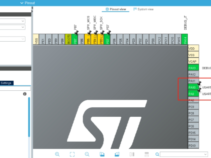
The STM32CubeMX configuration shown in the project uses SPI1 in full-duplex master mode with 8-bit transfers and MSB-first operation. The screenshots show PB3, PB4, and PB5 assigned to SPI1 SCK, MISO, and MOSI. The author also notes that internal pull-ups were enabled because the tested hardware lacked external pull-up resistors.
The firmware initializes the W5500-related GPIO, resets the Ethernet controller, sets the MAC address, allocates socket buffers, obtains network configuration, and then repeatedly services the TCP server.
The project reports an echo-test transfer rate of approximately 35.5 KB/s in the initial polling implementation. After changing the SPI path to DMA, the author reports that receive performance remained relatively slow while host-bound transmission increased to more than 200 KB/s. These numbers describe this particular firmware and test setup; they are far below the W5500 silicon's maximum network capability and should not be interpreted as W5500 throughput limits.
For product development, that observation is useful. A fast MCU alone does not guarantee high Ethernet throughput. Host-interface transactions, HAL overhead, copy operations, socket servicing, DMA strategy, buffer size, and application architecture can dominate actual performance.
Where WIZnet Fits
The source design uses the W5500 as a dedicated Ethernet/TCP/IP controller attached to STM32H750. The STM32 handles the application and controls sockets, while W5500 performs Ethernet and TCP/IP processing.
For a future STM32H7 commercial design, W6300 changes the host-side bandwidth and protocol capabilities significantly.
WIZnet specifies W6300 with:
hardware TCP/UDP and IPv4/IPv6 processing;
integrated 10/100 Ethernet MAC and PHY;
eight independent hardware sockets;
32 KB TX plus 32 KB RX socket memory;
QSPI and 8-bit parallel host interfaces;
up to approximately 91 Mbps measured network performance;
a 48-pin 7 × 7 mm package;
an industrial operating-temperature range of -40 °C to +85 °C.
For STM32H7, QSPI is the natural interface to evaluate first.
The original W5500 project uses three SPI data/clock signals plus chip select. A W6300 Quad-SPI design instead uses:
STM32H7 → QSPI CLK + NCS + IO0 + IO1 + IO2 + IO3 → W6300
W6300 defines QD0 and QD1 as MOSI/MISO in single-SPI operation and uses QD0 through QD3 as bidirectional data lines in Quad mode. Its MOD[3:0] = 0000 setting selects the QSPI host interface.
The current W6300 datasheet specifies a maximum SCLK of 75 MHz. Because Quad mode moves four data bits per data clock rather than one, it gives a substantially wider MCU-to-Ethernet-controller path than the W5500 SPI arrangement.
This matches STM32H7 hardware well. For example, STM32H750 devices provide a hardware Quad-SPI controller, and ST specifies the peripheral for operation up to 133 MHz under the applicable 3.3 V conditions. W6300's own timing limit would therefore determine the top QSPI clock in this pairing rather than the H750 peripheral maximum.
For a commercial product, this matters because the migration path is not:
W5500 → W6300 with the same SPI wiring
It is better treated as:
W5500 SPI prototype → W6300 QSPI product architecture
That allows the board and firmware to use the newer controller's host bandwidth rather than operating it as if it were simply another four-wire SPI peripheral.
Implementation Notes
Existing STM32H750 + W5500 Firmware
The following is real code published in the source article.
File: main.c
gpio_for_w5500_config();
reset_w5500();
set_w5500_mac();
socket_buf_init(txsize, rxsize);
IP_AutoSet(3500);
The sequence appears immediately after the STM32 GPIO, SPI, timer, and UART initialization. It configures the MCU-side W5500 signals, performs a hardware reset, sets the MAC address, allocates the W5500's eight socket buffers, and starts automatic network configuration.
The application then keeps the TCP server active with:
while (1)
{
    do_tcp_server();
}
This illustrates why WIZnet hardware offload fits the system architecture: the STM32 application services a hardware socket model instead of executing the TCP state machine itself.
Current Hardware Interface
The source CubeMX configuration establishes a useful prototype baseline:
STM32H750
PB3 → SPI1 SCK
PB4 → SPI1 MISO
PB5 → SPI1 MOSI
separate GPIO outputs are configured for W5500 control
SPI1 configured as full-duplex master
8-bit data
MSB first
CubeMX screenshot shows approximately 50 Mbit/s SPI configuration
The article does not expose enough source information to unambiguously map every displayed GPIO to W5500 CS and RESET, so assigning those two signals by inference would be inappropriate for a production schematic.
Commercial Migration to STM32H7 + W6300
For a new PCB, the W6300 QSPI interface should be planned around the following electrical groups.
| STM32H7 function | W6300 signal | W6300 pin | Purpose |
|---|---|---|---|
| QUADSPI CLK | SCLK | 30 | Host-interface clock |
| QUADSPI NCS | CSn | 29 | Chip select |
| QUADSPI IO0 | QD0 | 32 | QSPI data 0 |
| QUADSPI IO1 | QD1 | 33 | QSPI data 1 |
| QUADSPI IO2 | QD2 | 34 | QSPI data 2 |
| QUADSPI IO3 | QD3 | 35 | QSPI data 3 |
| GPIO output | RSTn | 46 | Hardware reset |
| EXTI-capable GPIO | INTn | 45 | Network/socket interrupt |
These signal definitions come directly from the W6300 pin description. WIZnet also publishes STM32 reference firmware for a W6300 design using a hardware QSPI peripheral, demonstrating the same CLK, NCS, IO0–IO3, RESET, and INT organization.
Several additional circuits are required around the chip before this becomes a production Ethernet design.
Clocking: W6300 requires a 25 MHz reference at XSCI/XSCO. The official module reference uses a 25 MHz crystal. The datasheet states that when an oscillator rather than a crystal is used, the oscillator feeds XSCI and XSCO remains unconnected.
Core power: W6300 operates from 3.3 V externally and generates a 1.2 V output at 1V2O. The datasheet requires the 1.2 V analog and digital supply pins to be powered from this output. The reference circuit uses local decoupling around these rails.
PHY bias: RSET_BG requires an external precision resistor to analog ground. The datasheet specifies 12.3 kΩ ±1%; the exact current reference circuit should be taken from the latest W6300 documentation when the PCB is frozen.
Interface selection: MOD[3:0] = 0000 selects QSPI. The eight DAT[7:0] pins belong to the parallel-bus interface and are unused in QSPI operation.
Reset: The WIZ630io reference schematic notes that the active-low reset signal should remain asserted for at least 700 µs. A commercial STM32 design should therefore generate a defined reset sequence rather than depend solely on startup timing.
Ethernet analog path: TXOP/TXON and RXIP/RXIN connect to Ethernet magnetics and the RJ45 path. The official WIZ630io schematic provides the transformer termination, 49.9 Ω network, shield coupling, crystal network, decoupling, and LED circuitry and is a more appropriate PCB starting point than copying the W5500 module wiring from the original prototype.
For a commercial board, the recommended top-level architecture is therefore:
STM32H7 application
↓
hardware QSPI + DMA
↓
W6300 TCP/IPv4/IPv6 offload
↓
integrated 10/100 PHY
↓
magnetics + RJ45 + ESD protection
↓
Ethernet network
The original project's SPI+DMA experiment is particularly relevant here. It already demonstrates that moving MCU-to-WIZnet transfers away from CPU polling improves host-side transmission. With W6300, designing the data path around QSPI and DMA from the beginning is preferable to treating DMA as a later optimization.
Practical Tips / Pitfalls
Route QSPI as a high-speed digital bus. CLK and QD0–QD3 should remain short, direct, and referenced to a continuous ground plane. Reserve locations for optional source-series resistors during the first prototype spin so edge-rate problems can be tuned after measurement.
Design from the W6300 reference Ethernet circuit. W6300 has different power, clock, interface, and PHY requirements from a W5500 module. The official W6300 reference schematic or WIZ630io circuit is a stronger production baseline than transplanting the old W5500 connector section.
Separate 3.3 V distribution from 1.2 V core distribution clearly in the schematic. W6300's 1V2O output supplies its 1.2 V domains. Place local decoupling close to the corresponding pins and follow the reference layout for analog and digital supply treatment.
Treat the magnetics/RJ45 area as an EMC boundary. Keep Ethernet differential pairs compact and symmetrical, place the magnetics close to the connector, provide an intentional chassis/shield strategy, and include an ESD solution appropriate to the product's regulatory environment.
Connect both RSTn and INTn to the STM32H7. Hardware reset provides deterministic recovery, while INTn allows socket and network events to be serviced without constant register polling. This is more suitable for a commercial firmware architecture than a permanent polling loop.
Benchmark QSPI DMA early. WIZnet lists W6300 network performance up to about 91 Mbps, but reaching high application throughput requires the STM32 memory, DMA, QSPI driver, socket buffers, and application framing to keep the controller supplied with data.
Plan compliance testing during PCB design. WIZnet's current W6300 documentation provides evaluation-board schematics and hardware resources, while several chip-level compliance resources are still marked as pending. Product-level ESD, radiated/conducted emissions, immunity, cable testing, thermal behavior, and Ethernet interoperability therefore remain responsibilities of the final system design.
FAQ
Q: Why choose W6300 for a future STM32H7 commercial product?
A: The main reasons are host-interface bandwidth and protocol longevity. W6300 combines hardware TCP/UDP processing, IPv4/IPv6 dual-stack support, eight sockets, 64 KB of combined TX/RX socket memory, and a four-data-line QSPI interface. WIZnet reports network performance up to approximately 91 Mbps, making it better aligned with high-performance STM32H7 designs than using a high-end MCU behind a narrow network-controller interface.
Q: How should W6300 connect to an STM32H7?
A: For a performance-oriented design, use the STM32H7 hardware Quad-SPI peripheral: CLK to SCLK, NCS to CSn, and four bidirectional IO signals to QD0–QD3. Add dedicated GPIOs for RSTn and INTn. On STM32H750, the Quad-SPI peripheral itself supports clock rates beyond the W6300's 75 MHz QSPI limit, so the interface can be designed around the W6300 timing specification.
Q: What role would W6300 play in this product architecture?
A: It would replace the W5500 used in the source prototype as the dedicated Ethernet/TCP/IP offload controller. STM32H7 would run the application, data processing, security, UI, storage, fieldbus, or other product-specific workloads, while W6300 would manage the Ethernet MAC/PHY and hardware TCP/UDP sockets for IPv4 and IPv6 networking.
Q: Can this design be used by developers without Ethernet PHY design experience?
A: The MCU-to-W6300 QSPI portion is accessible to an embedded developer familiar with STM32CubeMX, DMA, GPIO interrupts, and socket programming. A commercial PCB still requires more hardware discipline than a development-board project: power integrity, the 25 MHz clock, PHY bias components, magnetics, differential routing, connector shielding, ESD protection, and EMC validation all matter. Starting from WIZnet's reference schematic substantially reduces uncertainty.
Q: What changes when moving from the source project's W5500 to W6300?
A: The application concept remains similar—an STM32 controls hardware sockets in a WIZnet Ethernet controller—but the hardware interface should be redesigned around QSPI rather than merely reusing the W5500's SPI nets. W6300 adds QD2 and QD3, different mode-selection and power requirements, a 25 MHz clock circuit, 64 KB of combined TX/RX memory, IPv6 hardware support, and a higher-performance host architecture. Firmware can continue to use WIZnet's MCU-independent ioLibrary family, but the low-level host-interface functions must target the W6300 QSPI transaction format.
Source
Original Project: CSDN, “STM32H750驱动W5500”. The article was originally published in March 2023 and demonstrates W5500 TCP-server operation on STM32H750 using both SPI polling and SPI+DMA. It is published under CC BY-SA 4.0.
Original STM32H750 + W5500 article
W6300 Hardware Reference: WIZnet W6300 documentation, datasheet, pin definitions, QSPI timing, reference schematics, and socket-memory architecture.
STM32H7 Reference: STMicroelectronics STM32H750 documentation. STM32H750 provides a 480 MHz Cortex-M7, up to 1 MB RAM, and a hardware Quad-SPI interface specified up to 133 MHz under the documented electrical conditions.
Tags
#W6300 #W5500 #STM32H7 #STM32H750 #QSPI #Ethernet #TCPIP #IPv6 #HardwareDesign #PCBDesign #CommercialProduct #EmbeddedEthernet
상용 제품을 위한 STM32H7 + W6300 이더넷 하드웨어는 어떻게 설계할까?
요약
원본 프로젝트는 STM32H750과 WIZnet W5500을 SPI로 연결하고, DHCP 및 TCP 서버를 구현하면서 일반 SPI Polling 방식과 SPI+DMA 방식을 비교합니다. 향후 상용 STM32H7 제품에서는 이 구조를 W6300 기반으로 확장할 수 있습니다. 이 경우 기존 W5500의 4-wire SPI 대신 QSPI를 활용할 수 있으며, 하드웨어 IPv4/IPv6, 총 64 KB의 Socket TX/RX 메모리, WIZnet 기준 약 91 Mbps 수준의 네트워크 성능을 활용할 수 있습니다. 따라서 제품 설계 시에는 단순히 Ethernet Controller만 교체하는 것이 아니라 MCU Interface, Clock, Power, PHY Routing, Reset/Interrupt, EMC까지 포함해 전체 하드웨어 구조를 다시 설계하는 것이 적절합니다.
프로젝트가 하는 일
원본 CSDN 프로젝트는 STM32H750 + W5500으로 TCP Server를 구현하고 DHCP를 통해 IP를 자동으로 할당받는 구조입니다.
Host Interface는 두 가지 방식으로 시험합니다.
- 일반 SPI Polling
- SPI + DMA
STM32CubeMX 설정에서는 SPI1을 Full-Duplex Master로 구성하며 8-bit 전송과 MSB First 방식을 사용합니다.
프로젝트에 표시된 SPI1 핀은 다음과 같습니다.
- PB3 → SPI1 SCK
- PB4 → SPI1 MISO
- PB5 → SPI1 MOSI
작성자는 테스트 보드에 External Pull-up이 없는 부분을 보완하기 위해 일부 GPIO에서 Internal Pull-up도 설정했다고 설명합니다.
Firmware에서는 다음 순서로 W5500 Network Interface를 초기화합니다.
GPIO 설정 → W5500 Reset → MAC Address 설정 → Socket Buffer 설정 → DHCP/IP 설정 → TCP Server 실행
초기 Polling 방식의 Echo Test에서는 약 35.5 KB/s 수준의 전송 결과가 보고됩니다.
SPI를 DMA 방식으로 변경한 뒤에는 수신 성능 개선은 제한적이었지만 PC 방향의 송신 속도는 200 KB/s 이상으로 증가했다고 작성자가 설명합니다.
이 수치는 W5500 자체의 성능 한계가 아닙니다.
이 프로젝트에서 측정된 결과는 다음 요소에 영향을 받습니다.
- HAL 호출 Overhead
- SPI Transaction 구조
- DMA 사용 방식
- Socket Polling
- Buffer 크기
- Memory Copy
- Application Loop 구조
따라서 STM32H7처럼 빠른 MCU를 사용하더라도 Network Controller와 연결되는 Host Interface가 충분히 효율적이지 않으면 전체 Ethernet 성능은 낮게 나타날 수 있습니다.
WIZnet이 들어가는 위치
원본 설계에서 W5500은 STM32H750에 연결되는 전용 Ethernet/TCP/IP Controller입니다.
STM32는 Application Logic과 Socket Control을 담당하고 W5500은 Ethernet 및 TCP/IP 처리를 수행합니다.
향후 STM32H7 기반 상용 제품을 개발한다면 W6300은 이 구조를 한 단계 확장할 수 있습니다.
W6300은 다음 기능을 제공합니다.
- Hardware TCP/UDP
- Hardware IPv4/IPv6
- 10/100 Ethernet MAC/PHY
- 8 Hardware Sockets
- 32 KB TX + 32 KB RX Socket Memory
- QSPI Host Interface
- 8-bit Parallel Host Interface
- 약 91 Mbps 수준의 Network Performance
- 산업용 온도 범위 지원
STM32H7과 조합할 경우 우선 검토할 만한 Interface는 QSPI입니다.
기존 W5500은 보통 다음 구조입니다.
STM32H7 → SCLK / MOSI / MISO / CS → W5500
W6300을 Quad-SPI로 사용할 경우 구조는 다음과 같습니다.
STM32H7 → QSPI CLK / NCS / IO0 / IO1 / IO2 / IO3 → W6300
W6300에서는 QD0과 QD1을 Single SPI에서 MOSI/MISO로 사용할 수 있으며 Quad Mode에서는 QD0~QD3 네 선을 모두 Data Line으로 사용합니다.
QSPI Mode를 사용하는 경우 W6300의 Mode 설정은 해당 Host Interface 설정에 맞춰 구성해야 합니다.
W6300의 최대 SCLK는 현재 Datasheet 기준 75 MHz입니다.
Quad Mode에서는 한 Clock에 4 bit를 전달할 수 있기 때문에 기존 Single-SPI 기반 W5500보다 MCU와 Ethernet Controller 사이의 Host Interface Bandwidth를 크게 늘릴 수 있습니다.
STM32H750 자체는 W6300보다 높은 QSPI Clock을 지원할 수 있으므로 실제 조합에서는 W6300의 Timing Specification이 상한선이 됩니다.
따라서 상용 제품 Migration은 단순히 다음처럼 접근하는 것보다:
W5500 → W6300으로 Chip만 교체
다음과 같이 보는 것이 더 적절합니다.
W5500 SPI Prototype → W6300 QSPI Product Architecture
이렇게 해야 W6300의 Host Interface 성능을 제대로 활용할 수 있습니다.
구현 참고 사항
기존 STM32H750 + W5500 Firmware
원본 프로젝트에 실제로 포함된 초기화 흐름은 다음과 같습니다.
파일: main.c
gpio_for_w5500_config();
reset_w5500();
set_w5500_mac();
socket_buf_init(txsize, rxsize);
IP_AutoSet(3500);
이 코드는 STM32의 GPIO, SPI, Timer, UART 초기화 이후 실행됩니다.
각 함수의 역할은 다음과 같습니다.
- W5500 제어 GPIO 설정
- W5500 Hardware Reset
- MAC Address 설정
- Socket TX/RX Buffer 구성
- 자동 Network Configuration
이후 Main Loop에서는 TCP Server를 지속적으로 실행합니다.
while (1)
{
    do_tcp_server();
}
이 구조는 WIZnet Hardware Offload 방식의 특징을 잘 보여줍니다.
STM32가 TCP State Machine 자체를 실행하는 것이 아니라 W5500의 Hardware Socket을 제어하는 Application 구조입니다.
현재 W5500 Hardware Interface
원본 CubeMX 구성에서 확인 가능한 기본 연결은 다음과 같습니다.
STM32H750
- PB3 → SPI1 SCK
- PB4 → SPI1 MISO
- PB5 → SPI1 MOSI
- W5500 Control용 별도 GPIO
- SPI1 Full-Duplex Master
- 8-bit Data
- MSB First
CubeMX 화면에서는 약 50 Mbit/s 수준의 SPI 설정도 확인됩니다.
다만 공개된 자료만으로는 표시된 모든 GPIO를 W5500의 CS와 RESET에 정확하게 대응시키기 어렵습니다.
따라서 이 부분은 상용 회로도에 그대로 복사하기보다 새 제품의 MCU Pin Planning에 맞춰 다시 지정해야 합니다.
STM32H7 + W6300 상용 설계로 전환
새 PCB에서는 W6300 QSPI Interface를 다음과 같이 계획할 수 있습니다.
| STM32H7 기능 | W6300 Signal | W6300 Pin | 역할 |
|---|---|---|---|
| QUADSPI CLK | SCLK | 30 | Host Interface Clock |
| QUADSPI NCS | CSn | 29 | Chip Select |
| QUADSPI IO0 | QD0 | 32 | QSPI Data 0 |
| QUADSPI IO1 | QD1 | 33 | QSPI Data 1 |
| QUADSPI IO2 | QD2 | 34 | QSPI Data 2 |
| QUADSPI IO3 | QD3 | 35 | QSPI Data 3 |
| GPIO Output | RSTn | 46 | Hardware Reset |
| EXTI GPIO | INTn | 45 | Network/Socket Interrupt |
이 구조 외에도 실제 제품에서는 다음 회로가 추가로 필요합니다.
25 MHz Clock
W6300은 XSCI/XSCO에 사용하는 25 MHz Reference Clock이 필요합니다.
Crystal을 사용하는 경우 WIZnet Reference Circuit을 기준으로 Load Capacitor와 배치를 구성하는 것이 안전합니다.
외부 Oscillator를 사용하는 경우에는 XSCI에 Clock을 넣고 XSCO는 Datasheet 권장 연결 방식을 따라야 합니다.
상용 PCB에서는 Clock Trace를 짧게 유지하고 Ethernet Differential Pair와 같은 민감한 영역과의 Coupling을 줄이는 것이 중요합니다.
3.3 V와 1.2 V 전원
W6300은 외부에서 3.3 V를 공급받으며 내부에서 1.2 V Rail을 생성하는 구조를 사용합니다.
1V2O 출력은 W6300 내부의 1.2 V Analog/Digital Domain에 사용됩니다.
따라서 회로도에서는 다음 전원 Domain을 명확하게 분리하는 것이 좋습니다.
3.3 V Input → W6300 → 1V2O → Internal 1.2 V Domain
각 Power Pin 근처에는 Reference Design에 맞는 Decoupling Capacitor를 최대한 가깝게 배치해야 합니다.
PHY Bias
W6300의 RSET_BG에는 외부 Precision Resistor가 필요합니다.
현재 Datasheet에서는 12.3 kΩ ±1% 수준의 저항값을 지정합니다.
이 저항은 PHY Analog 특성에 관여하므로 일반 GPIO Pull-up처럼 임의값을 적용하기보다 Datasheet와 최신 Reference Schematic의 값을 그대로 따르는 것이 적절합니다.
Host Interface Mode
QSPI를 사용하는 경우 Mode Pin을 W6300의 QSPI 설정에 맞게 구성해야 합니다.
Parallel Bus를 사용하지 않는다면 DAT[7:0]은 QSPI 동작에 필요하지 않습니다.
제품 설계 초기에 다음을 명확히 결정하는 것이 좋습니다.
QSPI 제품인지, Parallel Bus 제품인지
둘 다 사용할 수 있도록 애매하게 설계하면 Pin Count와 Routing Complexity만 증가할 수 있습니다.
Reset
W6300은 Active-Low Reset인 RSTn을 제공합니다.
상용 제품에서는 MCU GPIO를 연결해 Firmware에서 강제로 Network Controller를 Reset할 수 있도록 하는 것이 좋습니다.
이를 통해 다음 상황에서 Recovery가 가능합니다.
- Network Controller Lock-up
- Abnormal Power Sequence
- Firmware Watchdog Recovery
- Cable/Network Error 이후 재초기화
Reference Design에서는 충분한 Reset Pulse Width를 확보하도록 요구하므로 STM32 Boot 직후 즉시 Reset을 해제하는 방식보다 명확한 Power-up Sequence를 구성하는 것이 안전합니다.
Ethernet PHY와 RJ45
W6300의 Ethernet Differential Signal은 다음과 같습니다.
- TXOP / TXON
- RXIP / RXIN
이 신호는 Magnetics를 거쳐 RJ45 Connector로 연결됩니다.
상용 제품에서는 W6300부터 RJ45까지의 구간을 단순한 Digital Signal Routing으로 보면 안 됩니다.
다음 항목을 함께 설계해야 합니다.
- Transformer / Magnetics
- 49.9 Ω Termination Network
- Common-mode 특성
- RJ45 Shield
- Chassis Ground Strategy
- ESD Protection
- Differential Pair Routing
WIZ630io Reference Schematic은 이 부분의 좋은 출발점입니다.
최종 구조는 다음과 같이 정리할 수 있습니다.
STM32H7 Application
↓
Hardware QSPI + DMA
↓
W6300 Hardware TCP/IPv4/IPv6 Offload
↓
10/100 Ethernet PHY
↓
Magnetics + RJ45 + ESD Protection
↓
Ethernet Network
원본 프로젝트에서 SPI Polling을 DMA 방식으로 변경했을 때 Host-side Transmission Performance가 개선됐다는 점도 중요한 참고가 됩니다.
W6300 기반 제품에서는 DMA를 나중에 추가하는 최적화 기능으로 보기보다 처음부터 다음 구조로 설계하는 것이 좋습니다.
Application Buffer → DMA → QSPI → W6300 Socket Buffer
실무 설계 팁 / 주의점
- QSPI는 일반 저속 GPIO처럼 배선하면 안 됩니다. CLK와 QD0~QD3는 짧고 직접적으로 배치하고 연속적인 Ground Plane 위에서 Routing하는 것이 좋습니다. 첫 번째 Prototype에는 필요 시 Source Series Resistor를 넣을 수 있도록 Option Pad를 준비하면 Signal Integrity Debug에 도움이 됩니다.
- Ethernet 회로는 W6300 Reference Design에서 시작하는 것이 안전합니다. W5500 Module 회로를 그대로 복사하기보다 W6300 전용 Power, Clock, PHY, Magnetics 구조를 기준으로 설계해야 합니다.
- 3.3 V와 1.2 V Domain을 회로도에서 명확하게 구분해야 합니다.
1V2O와 관련된 Decoupling은 W6300 가까이에 배치하고 Analog/Digital Supply Routing은 Reference Layout을 따르는 것이 좋습니다. - Magnetics와 RJ45 주변을 EMC Boundary로 설계해야 합니다. Differential Pair, Connector Shield, Chassis Ground, ESD Protection을 제품 인증 단계가 아니라 PCB 설계 단계부터 함께 고려해야 합니다.
- RSTn과 INTn을 모두 STM32H7에 연결하는 것이 좋습니다. Reset은 Network Controller Recovery에 필요하고 Interrupt는 Socket 상태를 무한 Polling하는 방식보다 효율적인 Firmware 구조를 만들 수 있습니다.
- QSPI DMA 성능을 초기 Prototype 단계에서 측정해야 합니다. W6300 자체가 높은 Network Performance를 지원하더라도 STM32 Memory, DMA, QSPI Driver, Buffer Allocation이 병목이면 Application Throughput은 낮아질 수 있습니다.
- 제품 인증을 PCB 설계 단계부터 고려하는 것이 좋습니다. Ethernet 제품은 ESD, Radiated/Conducted Emission, Immunity, Cable Test, Thermal Test, Link Interoperability까지 최종 제품에서 검증해야 합니다.
FAQ
Q: 향후 STM32H7 상용 제품에 왜 W6300을 선택할 수 있나요?
A: W6300은 Hardware TCP/UDP, IPv4/IPv6 Dual Stack, 8개의 Socket, 총 64 KB의 TX/RX Socket Memory, QSPI Host Interface를 제공합니다. 특히 STM32H7처럼 높은 처리 성능을 가진 MCU에서는 W5500의 Single-SPI 구조보다 QSPI 기반 Host Interface를 활용하는 것이 전체 Network Architecture에 더 잘 맞을 수 있습니다.
Q: W6300은 STM32H7과 어떻게 연결하는 것이 좋나요?
A: 성능을 중요하게 보는 제품이라면 STM32H7의 Hardware Quad-SPI를 사용하는 것이 적절합니다. CLK는 SCLK, NCS는 CSn, IO0~IO3는 W6300의 QD0~QD3에 연결하고 별도의 GPIO를 RSTn과 INTn에 할당합니다. W6300 최대 QSPI Clock은 75 MHz이므로 STM32H7 QSPI Peripheral 설정도 이 Timing Limit 안에서 구성해야 합니다.
Q: 이 제품 구조에서 W6300은 어떤 역할을 하나요?
A: 원본 프로젝트의 W5500을 대체하는 Hardware Ethernet/TCP/IP Offload Controller 역할을 합니다. STM32H7은 Application, Data Processing, UI, Storage, Fieldbus 또는 제품 고유 기능을 처리하고 W6300은 Ethernet MAC/PHY와 Hardware TCP/UDP Socket, IPv4/IPv6 통신을 담당합니다.
Q: Ethernet PHY 설계 경험이 적은 개발자도 W6300 상용 보드를 설계할 수 있나요?
A: STM32H7과 W6300 사이의 QSPI 부분은 STM32CubeMX, DMA, GPIO Interrupt, Socket Programming 경험이 있다면 비교적 접근하기 쉽습니다. 다만 상용 PCB에서는 25 MHz Clock, Power Integrity, PHY Bias, Magnetics, Differential Routing, RJ45 Shield, ESD, EMC까지 고려해야 하므로 WIZnet Reference Schematic과 Layout을 기준으로 설계하는 것이 중요합니다.
Q: 기존 W5500 설계에서 W6300으로 변경할 때 가장 큰 차이는 무엇인가요?
A: Application 관점에서는 둘 다 WIZnet Hardware Socket을 사용하는 구조이지만 Hardware Interface는 새로 설계하는 것이 좋습니다. W6300에서는 QSPI를 사용할 수 있기 때문에 QD2/QD3가 추가되고, Mode Setting, 25 MHz Clock, Power 구조, 64 KB Socket Memory, IPv6 Hardware Support 등을 고려해야 합니다. Firmware에서도 상위 Socket 구조는 유사하게 유지할 수 있지만 Low-Level Host Interface는 W6300 QSPI Transaction에 맞춰야 합니다.
출처
Original Project: CSDN, “STM32H750驱动W5500”
2023년 3월 공개된 STM32H750 + W5500 프로젝트로, W5500 TCP Server와 SPI Polling 및 SPI+DMA 방식을 다룹니다.
License: CC BY-SA 4.0
W6300 Hardware Reference: WIZnet W6300 공식 문서, Datasheet, Reference Schematic 및 WIZ630io Hardware 자료
STM32H7 Reference: STMicroelectronics STM32H750 Datasheet 및 Product Documentation
태그
#W6300 #W5500 #STM32H7 #STM32H750 #QSPI #Ethernet #TCPIP #IPv6 #HardwareDesign #PCBDesign #CommercialProduct #EmbeddedEthernet