
How to Design a Standalone W5500 Ethernet PCB Module for Makers and Education?
This project analyzes the hardware PCB design of a standalone W5500 Ethernet network module without MCU integration.
How to Design a Standalone W5500 Ethernet PCB Module for Makers and Education?
(메이커와 교육을 위한 독립형 W5500 이더넷 PCB 모듈 설계 방법)
Project Summary (56 words)
This project analyzes the hardware PCB design of a standalone W5500 Ethernet network module without MCU integration. By implementing proper power regulation, differential Ethernet routing, clock stability, and SPI breakout design, the module becomes a reusable and educational reference for makers learning real Ethernet hardware development.
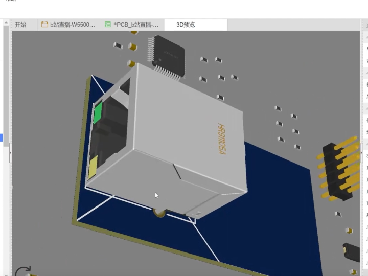
Hardware Architecture Overview
A standalone W5500 module includes four essential design blocks:
1️⃣ Power Section
3.3 V regulated supply
Multiple 0.1 µF decoupling capacitors per power pin
Bulk capacitor for supply stability
Short ground return paths
Stable power is essential for PHY operation.
2️⃣ Clock Circuit
25 MHz crystal oscillator
Matched load capacitors
Very short trace routing
Clock noise can lead to unstable Ethernet links.
3️⃣ Ethernet PHY Section
Differential pair routing (TX+/−, RX+/−)
100 Ω differential impedance
RJ45 with integrated magnetics
ESD protection diodes
This section determines overall link reliability.
4️⃣ SPI Interface Header
The module exposes:
MOSI
MISO
SCK
CS
RESET
INT
This modular design allows flexible MCU pairing.
PCB Design Best Practices
Use solid ground plane
Avoid routing high-speed signals over split planes
Keep differential pairs tightly coupled
Place magnetics close to RJ45
Isolate noisy power circuits
These practices align with professional Ethernet hardware design standards.
Why This Is Valuable for Makers
Many hobby boards hide Ethernet complexity. This module:
Exposes true Ethernet hardware structure
Teaches signal integrity fundamentals
Encourages modular hardware thinking
Bridges hobby electronics and industrial design
It is ideal for embedded hardware workshops and educational labs.
Industrial Design Perspective
Even in maker environments, following proper PCB discipline ensures:
Reliable long-term Ethernet operation
EMI/ESD resilience
Stable PHY negotiation
Reduced debugging effort
The same principles apply to industrial IoT hardware.
FAQ (WIZnet-Focused)
Q1: Why design a standalone W5500 PCB instead of using a shield?
A: Designing the PCB teaches real Ethernet layout rules and provides full control over signal integrity and power routing.
Q2: What impedance should Ethernet differential pairs have?
A: Typically 100 Ω differential impedance for proper signal integrity.
Q3: How important is the crystal placement?
A: Very important. It must be placed close to W5500 with short symmetric traces.
Q4: Can this module be reused with different MCUs?
A: Yes. The SPI breakout allows flexible integration.
Q5: Is this design suitable for professional use?
A: Yes, if PCB layout, grounding, and EMI considerations are implemented correctly.
Tags
#W5500 #EthernetPCB #HardwareDesign #PCBLayout #EmbeddedEducation #MakerProject
🇰🇷 KOREAN VERSION
메이커와 교육을 위한 독립형 W5500 이더넷 PCB 모듈을 설계하는 방법은?
(How to Design a Standalone W5500 Ethernet PCB Module for Makers and Education?)
프로젝트 개요 (56단어)
이 프로젝트는 MCU 없이 W5500 기반 이더넷 네트워크 모듈의 PCB 설계를 분석합니다. 전원 안정화, 차동 신호 라우팅, 클럭 회로 설계, SPI 인터페이스 분리 설계를 통해 메이커와 학생들이 실제 이더넷 하드웨어 설계 원리를 학습할 수 있는 교육용 레퍼런스를 제공합니다.
하드웨어 구성 요소
1. 전원 설계
3.3V 레귤레이터
디커플링 캐패시터 다중 배치
안정적인 그라운드 설계
2. 클럭 회로
25MHz 크리스탈
짧은 배선
정확한 부하 캐패시턴스
3. 이더넷 PHY 영역
100Ω 차동 임피던스
RJ45 + 마그네틱
ESD 보호
4. SPI 인터페이스
MOSI / MISO / SCK / CS
RESET / INT
다양한 MCU와 연결 가능한 모듈형 구조입니다.
교육적 가치
이 설계는:
이더넷 하드웨어 이해
PCB 신호 무결성 학습
산업용 설계 기준 체험
에 매우 적합합니다.
FAQ
Q1: 왜 독립형 PCB를 설계하나요?
A: 실제 이더넷 설계 원리를 배우기 위해서입니다.
Q2: 차동 임피던스는 얼마인가요?
A: 일반적으로 100Ω입니다.
Q3: 크리스탈 배치가 중요한가요?
A: 매우 중요합니다. 신호 안정성에 직접적 영향을 줍니다.
Q4: 다른 MCU와 연결 가능한가요?
A: 네, SPI 인터페이스로 연결 가능합니다.
Q5: 산업용으로 사용 가능한가요?
A: 적절한 PCB 설계 시 가능합니다.