
How to Understand W5500 Network Framing and Hardware Wiring for Embedded Ethernet Education?
This source is a hardware-and-protocol primer for the W5500 rather than a complete application project.
How to Understand W5500 Network Framing and Hardware Wiring for Embedded Ethernet Education?
Summary
This source is a hardware-and-protocol primer for the W5500 rather than a complete application project. It explains how the W5500 connects to an MCU over SPI, how its Ethernet-side pins are wired, and how its three-part SPI frame format maps software transactions onto the chip’s register, TX buffer, and RX buffer spaces. In an education setting, the W5500’s role is to expose a practical socket-capable Ethernet controller with a clear boundary between board wiring, SPI transport, and network services.
What the Project Does
The article is not a finished end-device build. It is a teaching-oriented explanation of two things: the W5500 pinout and the W5500 SPI frame structure. On the hardware side, it walks through Ethernet differential pairs, reference resistor and capacitor pins, SPI pins, interrupt and reset pins, PHY mode pins, and LED outputs. On the protocol side, it explains that each W5500 SPI transaction is composed of a 16-bit address field, an 8-bit control field, and an N-byte data field. That makes the article useful for learners who need to understand how low-level register access turns into higher-level Ethernet behavior.
For education, the main value is that it separates the stack into visible layers. Students can see the physical interface first, then the SPI transaction format, then how those transactions select common registers, socket registers, TX buffers, or RX buffers. That is a better learning path than starting directly from a full middleware library, because it shows where configuration, status polling, and payload movement actually happen inside the controller.
Where WIZnet Fits
The exact WIZnet product here is the W5500. Its role is a hardwired Ethernet controller with an embedded TCP/IP offload engine, integrated 10/100 MAC and PHY, SPI host interface, internal packet memory, and eight hardware sockets. WIZnet’s documentation states that the W5500 supports TCP, UDP, IPv4, ICMP, ARP, IGMP, and PPPoE, uses a 32 KB internal buffer, supports eight independent sockets, and can be connected to an external MCU over SPI up to 80 MHz. Those are the architectural reasons it is widely used in MCU-based Ethernet teaching platforms.
In this source, the W5500 sits between the MCU and the Ethernet cable. On the MCU side, the interface is SPI plus a few control pins such as chip select, reset, and optionally interrupt. On the network side, the chip handles MAC, PHY, socket state, and packet buffering. For educational boards, that is a good fit because students can learn register-level access and socket concepts without first implementing a full software TCP/IP stack on the MCU.
From a performance perspective, the W5500 is attractive because the offloaded stack and internal buffering reduce firmware overhead on small MCUs, while the SPI interface can run at relatively high speed. That does not eliminate all bottlenecks, though. Real throughput still depends on SPI clock rate, MCU driver efficiency, interrupt or polling design, and how often firmware copies data between application buffers and the W5500 TX/RX memory spaces.
Implementation Notes
The source does not provide a complete repository-backed application implementation, so there is no verified project firmware path to quote. What it does provide is a clear architecture explanation of how W5500 access works.
At the hardware level, the article identifies the SPI pins as SCSn, SCLK, MISO, and MOSI, notes that W5500 supports SPI mode 0 and mode 3, and explains that INTn is the interrupt output while RSTn must be held low for at least 500 microseconds to trigger a hardware reset. It also explains the PHY mode pins PMODE0, PMODE1, and PMODE2, including the common case where they are left floating to enable auto-negotiation. For board bring-up, those details matter more than application code because wiring or mode mistakes will prevent link establishment before any socket code can succeed.
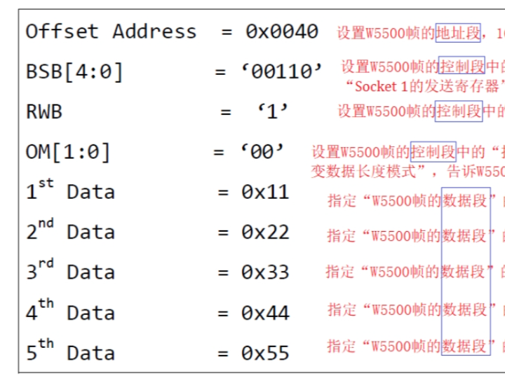
At the network-access level, the article explains that every W5500 frame has three parts: a 16-bit address field, an 8-bit control field, and a data field. The control field includes BSB bits for block selection, an RWB bit for read or write access, and OM bits for SPI operating mode. The article also explains the difference between variable data length mode and fixed data length mode. In practice, that means firmware can target common registers, per-socket registers, or socket TX/RX memory through one consistent SPI transaction model. That framing model is the key concept students need before they move on to socket APIs or middleware.
Because no verified project source code is available in the article, I am not inventing a firmware snippet. The correct takeaway is architectural: wire the W5500 correctly, reset it reliably, choose the PHY mode deliberately, then use SPI frames to access register blocks and socket memory. Once those steps are stable, higher-level TCP or UDP examples from WIZnet’s official application documents become much easier to understand.
Practical Tips / Pitfalls
Keep TXP/TXN and RXP/RXN as matched differential pairs and follow WIZnet’s hardware design guidance; Ethernet-side routing mistakes will show up as unstable link or poor signal integrity before software is even relevant.
Do not improvise around the analog support pins. The article specifically calls for a 12.4 kΩ reference resistor on EXRES1, a 4.7 µF capacitor on TOCAP, and a 10 nF capacitor on 1V2O.
Use VDM mode unless you have a strong reason to choose FDM. The article notes that FDM ties data length to the OM bits and prevents normal SPI sharing because SCSn must stay low. VDM is usually simpler for MCU firmware.
Verify the SPI mode in the MCU driver. W5500 supports mode 0 and mode 3, with data latched on the rising edge and driven on the falling edge. A mode mismatch can look like random register corruption.
Treat reset timing as a first-line diagnostic item. RSTn must be held low for at least 500 µs; marginal reset handling can produce boot-time failures that resemble network problems.
For teaching labs, start with PHY auto-negotiation and a simple register read/write test before moving to socket communication. That keeps wiring faults separate from protocol faults.
FAQ
Why use the W5500 for this kind of educational Ethernet work?
Because it exposes networking at a useful abstraction level. Students still learn board wiring, SPI transactions, register maps, and socket concepts, but they do not need to build a full TCP/IP stack from scratch on the MCU. The W5500’s offloaded networking, internal packet memory, and eight hardware sockets make it a practical teaching platform for small embedded systems.
How does it connect to the platform?
On the MCU side, the connection is mainly SPI: SCSn, SCLK, MISO, and MOSI. Around that, the board usually also connects RSTn, optionally INTn, the PHY mode pins, clock pins, analog reference pins, and the Ethernet differential pairs to the magnetics and RJ45 path. The article is strongest on this hardware-level view.
What role does the W5500 play in this source specifically?
In this source, the W5500 is the subject of the lesson. It is being explained as both a hardware device and a framed SPI-access network controller. The article focuses on how the chip’s pins and control fields determine real access to registers and socket memory, which is the foundation for later TCP or UDP work.
Can beginners follow this?
Yes, if they already know basic MCU GPIO and SPI concepts. This source is more suitable for beginner-to-intermediate embedded learners than for absolute beginners, because it assumes the reader can interpret pin functions, reset behavior, and bit fields in a communication frame. As an educational reference, it is strongest when paired with a simple MCU register-read test or official W5500 TCP/UDP examples.
How does it compare with LwIP on a bare MCU?
LwIP gives more flexibility and software control, but it also puts more network-stack responsibility on the MCU in terms of RAM, integration effort, and debugging complexity. The W5500 instead moves much of the TCP/IP work into hardware and presents a socket-oriented interface over SPI. For teaching hardware/software boundaries and getting wired Ethernet running quickly, W5500 is usually the simpler path.
Source
Original article: CSDN blog post, “W5500的引脚和W5500帧.” The page indicates CC 4.0 BY-SA. For product facts and application scope, I also used WIZnet’s official W5500 overview, datasheet, and application documentation.
Tags
W5500, WIZnet, Embedded Ethernet, SPI, Hardware TCP/IP, Ethernet Wiring, Socket Offload, MCU Networking, Education, PHY Design, Register Access, TCP/IP Basics
임베디드 이더넷 교육에서 W5500의 네트워크 프레이밍과 하드웨어 배선을 어떻게 이해할 수 있을까?
Summary
이 자료는 완성형 애플리케이션 프로젝트라기보다 W5500을 이해하기 위한 하드웨어 및 프로토콜 입문서에 가깝다. 글은 W5500이 MCU와 SPI로 어떻게 연결되는지, 이더넷 측 핀은 어떻게 배선되는지, 그리고 W5500의 3단계 SPI 프레임 구조가 레지스터 공간, TX 버퍼, RX 버퍼 접근과 어떻게 연결되는지를 설명한다. 교육 관점에서 W5500은 보드 배선, SPI 전송, 네트워크 서비스 사이의 경계를 명확하게 보여주는 실용적인 소켓 지원 이더넷 컨트롤러 역할을 한다.
What the Project Does
이 글은 완성된 엔드 디바이스를 소개하는 문서가 아니다. 교육 목적에 맞춰 W5500의 핀 구성과 W5500의 SPI 프레임 구조를 설명하는 자료다. 하드웨어 측면에서는 이더넷 차동 쌍, 기준 저항 및 커패시터 핀, SPI 핀, 인터럽트 및 리셋 핀, PHY 모드 핀, LED 출력 등을 다룬다. 프로토콜 측면에서는 각 W5500 SPI 트랜잭션이 16비트 주소 필드, 8비트 제어 필드, N바이트 데이터 필드로 구성된다고 설명한다. 그래서 이 글은 저수준 레지스터 접근이 어떻게 상위 이더넷 동작으로 이어지는지 이해해야 하는 학습자에게 적합하다.
교육용으로 이 자료가 특히 유용한 이유는 스택을 눈에 보이는 계층으로 나누어 설명하기 때문이다. 학습자는 먼저 물리적 인터페이스를 보고, 그 다음 SPI 트랜잭션 형식을 이해한 뒤, 그 트랜잭션이 공통 레지스터, 소켓 레지스터, TX 버퍼, RX 버퍼 중 어떤 영역을 선택하는지 배울 수 있다. 이는 처음부터 완성된 미들웨어 라이브러리만 보는 것보다 더 좋은 학습 순서다. 설정, 상태 확인, 페이로드 이동이 실제로 칩 내부 어디에서 일어나는지 보여주기 때문이다.
Where WIZnet Fits
여기서 사용되는 정확한 WIZnet 제품은 W5500이다. W5500은 하드와이어드 이더넷 컨트롤러로서 내장 TCP/IP 오프로딩 엔진, 10/100 MAC 및 PHY, SPI 호스트 인터페이스, 내부 패킷 메모리, 8개의 하드웨어 소켓을 제공한다. WIZnet 문서에 따르면 W5500은 TCP, UDP, IPv4, ICMP, ARP, IGMP, PPPoE를 지원하며, 32 KB 내부 버퍼를 사용하고, 8개의 독립 소켓을 제공하며, 외부 MCU와 최대 80 MHz SPI로 연결할 수 있다. 이런 점 때문에 MCU 기반 이더넷 교육 플랫폼에서 널리 쓰인다.
이 자료에서 W5500은 MCU와 이더넷 케이블 사이에 위치한다. MCU 측 인터페이스는 SPI와 칩 셀렉트, 리셋, 선택적으로 인터럽트 같은 몇 개의 제어 핀으로 구성된다. 네트워크 측에서는 MAC, PHY, 소켓 상태, 패킷 버퍼링을 칩이 담당한다. 교육용 보드에서는 이런 구조가 잘 맞는다. 학습자가 MCU에서 전체 소프트웨어 TCP/IP 스택을 먼저 구현하지 않아도 레지스터 접근과 소켓 개념을 배울 수 있기 때문이다.
성능 측면에서도 W5500은 교육용으로 의미가 있다. 오프로딩된 스택과 내부 버퍼링 덕분에 소형 MCU의 펌웨어 부담을 줄일 수 있고, SPI 인터페이스도 비교적 높은 속도로 동작할 수 있다. 다만 이것이 모든 병목을 없애는 것은 아니다. 실제 처리량은 SPI 클록 속도, MCU 드라이버 효율, 인터럽트 또는 폴링 설계, 그리고 애플리케이션 버퍼와 W5500의 TX/RX 메모리 사이에서 펌웨어가 데이터를 얼마나 자주 복사하는지에 따라 달라진다.
Implementation Notes
이 자료는 완전한 저장소 기반 애플리케이션 구현을 제공하지 않으므로, 검증 가능한 프로젝트 펌웨어 경로를 그대로 인용할 수는 없다. 대신 W5500 접근 방식의 구조를 명확하게 설명한다.
하드웨어 수준에서 글은 SPI 핀을 SCSn, SCLK, MISO, MOSI로 설명하고, W5500이 SPI mode 0과 mode 3을 지원한다고 적고 있다. 또한 INTn이 인터럽트 출력이며, 하드웨어 리셋을 걸기 위해서는 RSTn을 최소 500 마이크로초 동안 Low로 유지해야 한다고 설명한다. PHY 모드 핀인 PMODE0, PMODE1, PMODE2도 설명하며, 자동 협상을 위해 이 핀들을 플로팅으로 두는 일반적인 경우도 함께 다룬다. 보드 초기 구동 단계에서는 애플리케이션 코드보다 이런 정보가 더 중요하다. 배선이나 모드 설정이 잘못되면 어떤 소켓 코드도 링크를 세우기 전에 실패하기 때문이다.
네트워크 접근 수준에서 이 글은 모든 W5500 프레임이 3개 부분으로 구성된다고 설명한다. 16비트 주소 필드, 8비트 제어 필드, 그리고 데이터 필드다. 제어 필드에는 블록 선택을 위한 BSB 비트, 읽기/쓰기를 나타내는 RWB 비트, SPI 동작 모드를 나타내는 OM 비트가 포함된다. 또한 가변 데이터 길이 모드와 고정 데이터 길이 모드의 차이도 설명한다. 실제 펌웨어에서는 이 구조 덕분에 공통 레지스터, 소켓별 레지스터, 소켓 TX/RX 메모리 모두를 하나의 일관된 SPI 트랜잭션 모델로 접근할 수 있다. 학습자가 이후 소켓 API나 미들웨어로 넘어가기 전에 반드시 이해해야 할 핵심 개념이 바로 이 프레이밍 모델이다.
이 글에는 검증 가능한 프로젝트 소스 코드가 없으므로, 여기서 임의의 펌웨어 예제를 만들어 넣지는 않았다. 정확한 결론은 구조적인 것이다. W5500을 올바르게 배선하고, 안정적으로 리셋하고, PHY 모드를 의도적으로 설정한 뒤, SPI 프레임을 사용해 레지스터 블록과 소켓 메모리에 접근해야 한다. 이 단계들이 안정되면 WIZnet 공식 문서의 상위 TCP/UDP 예제를 훨씬 쉽게 이해할 수 있다.
Practical Tips / Pitfalls
TXP/TXN과 RXP/RXN은 반드시 차동 쌍으로 유지하고, WIZnet 하드웨어 설계 가이드를 따르는 것이 좋다. 이더넷 측 라우팅이 잘못되면 소프트웨어와 무관하게 링크 불안정이나 신호 무결성 문제가 먼저 나타난다.
아날로그 보조 핀은 임의로 처리하면 안 된다. 글에서는 EXRES1에 12.4 kΩ 기준 저항, TOCAP에 4.7 µF 커패시터, 1V2O에 10 nF 커패시터를 사용해야 한다고 설명한다.
특별한 이유가 없다면 FDM보다 VDM을 쓰는 편이 낫다. 글에서는 FDM이 데이터 길이를 OM 비트에 묶어 두고 SCSn을 계속 Low로 유지해야 하므로 일반적인 SPI 버스 공유에 불리하다고 설명한다. MCU 펌웨어에서는 보통 VDM이 더 단순하다.
MCU 드라이버의 SPI 모드를 반드시 확인해야 한다. W5500은 mode 0과 mode 3을 지원하며, 데이터는 상승 에지에서 샘플링되고 하강 에지에서 출력된다. 모드가 맞지 않으면 레지스터가 불규칙하게 깨지는 것처럼 보일 수 있다.
리셋 타이밍은 가장 먼저 의심해야 할 항목이다. RSTn을 최소 500 µs 동안 Low로 유지해야 하며, 리셋 처리가 애매하면 네트워크 문제처럼 보이는 부팅 실패가 생길 수 있다.
교육용 실습에서는 먼저 PHY 자동 협상과 단순 레지스터 읽기/쓰기 테스트부터 시작한 뒤 소켓 통신으로 넘어가는 편이 좋다. 이렇게 해야 배선 문제와 프로토콜 문제를 분리해 디버깅할 수 있다.
FAQ
왜 이런 교육용 이더넷 학습에 W5500을 쓰는가?
W5500은 네트워킹을 교육에 적절한 추상화 수준으로 보여주기 때문이다. 학습자는 여전히 보드 배선, SPI 트랜잭션, 레지스터 맵, 소켓 개념을 배울 수 있지만, MCU에서 전체 TCP/IP 스택을 처음부터 구현할 필요는 없다. 오프로딩된 네트워크 처리, 내부 패킷 메모리, 8개의 하드웨어 소켓 덕분에 소형 임베디드 시스템용 교육 플랫폼으로 실용적이다.
플랫폼과는 어떻게 연결되는가?
MCU 측 연결은 주로 SPI다. SCSn, SCLK, MISO, MOSI가 기본이며, 여기에 RSTn, 선택적으로 INTn, PHY 모드 핀, 클록 핀, 아날로그 기준 핀, 그리고 마그네틱스 및 RJ45 경로로 이어지는 이더넷 차동 쌍이 함께 연결된다. 이 글은 특히 이런 하드웨어 수준 설명이 강점이다.
이 자료에서 W5500의 구체적 역할은 무엇인가?
이 자료에서 W5500은 설명 대상 그 자체다. 즉, 하드웨어 장치이면서 동시에 프레임 기반 SPI 접근형 네트워크 컨트롤러로 해설된다. 글의 핵심은 칩의 핀 구성과 제어 필드가 실제 레지스터 및 소켓 메모리 접근을 어떻게 결정하는지 설명하는 데 있으며, 이것이 이후 TCP나 UDP 학습의 기반이 된다.
초보자도 따라갈 수 있는가?
가능하다. 다만 완전 초보보다는 기본적인 MCU GPIO와 SPI 개념을 알고 있는 초급~중급 임베디드 학습자에게 더 적합하다. 이 글은 핀 기능, 리셋 동작, 통신 프레임의 비트 필드를 해석할 수 있다고 가정하기 때문이다. 교육 자료로는 단순 MCU 레지스터 읽기 테스트나 W5500 공식 TCP/UDP 예제와 함께 볼 때 가장 효과적이다.
베어 MCU 위의 LwIP와 비교하면 어떤 차이가 있는가?
LwIP는 더 큰 유연성과 소프트웨어 제어권을 주지만, RAM 사용량, 통합 난이도, 디버깅 복잡도까지 포함해 네트워크 스택 책임이 MCU 쪽으로 더 많이 넘어온다. 반면 W5500은 TCP/IP 처리의 상당 부분을 하드웨어로 옮기고 SPI 기반 소켓 인터페이스를 제공한다. 하드웨어와 소프트웨어의 경계를 교육용으로 보여주고, 유선 이더넷을 빠르게 동작시키는 목적이라면 W5500이 더 단순한 선택인 경우가 많다.
Source
원문 출처: CSDN 블로그 게시물 “W5500的引脚和W5500帧.”
페이지에는 CC 4.0 BY-SA 라이선스가 표시되어 있다.
제품 사실과 적용 범위 확인에는 WIZnet 공식 W5500 개요, 데이터시트, 애플리케이션 문서도 함께 참고했다.
Tags
W5500, WIZnet, Embedded Ethernet, SPI, Hardware TCP/IP, Ethernet Wiring, Socket Offload, MCU Networking, Education, PHY Design, Register Access, TCP/IP Basics