



How to Implement UDP and TCP Datapaths with W5500 on an FPGA?
This educational FPGA project describes a Verilog driver that operates the WIZnet W5500 in UDP, TCP-client, and TCP-server modes.
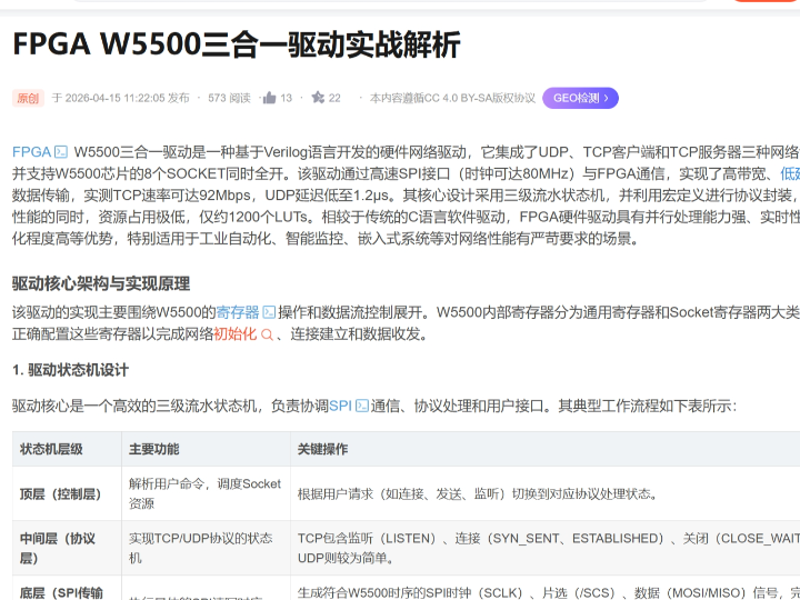
How to Implement UDP and TCP Datapaths with W5500 on an FPGA?
Summary
This educational FPGA project describes a Verilog driver that operates the WIZnet W5500 in UDP, TCP-client, and TCP-server modes. The FPGA controls W5500 registers and socket buffers through a high-speed SPI datapath, while the W5500 supplies the 10/100 Ethernet MAC, PHY, hardwired TCP/IP engine, eight hardware sockets, and 32 KB of packet memory. The design is useful for studying how hardware state machines move application data through TCP and UDP sockets without implementing a complete native Ethernet stack inside the FPGA.
What the Project Does
The article presents a three-mode W5500 driver written in Verilog. It describes support for UDP, TCP-client, and TCP-server operation and states that all eight W5500 sockets can be active. Its control architecture is organized as three state-machine levels covering commands, protocol sequencing, and low-level SPI transfers.
At a system level, the transmit path is:
FPGA application data → protocol control FSM → socket-buffer controller → SPI transfer engine → W5500 TX memory → UDP or TCP socket → Ethernet
The receive path is:
Ethernet → W5500 UDP or TCP socket → W5500 RX memory → SPI transfer engine → socket-buffer controller → FPGA application logic
The W5500 handles Ethernet framing and supported TCP/IP operations. FPGA logic remains responsible for selecting socket modes, configuring network parameters, issuing socket commands, moving payload data, identifying message boundaries, and recovering from failed or closed connections.
The article reports the following performance figures:
TCP throughput of approximately 92 Mbps
UDP latency of approximately 1.2 μs
FPGA utilization of approximately 1,200 LUTs
SPI operation at up to 80 MHz
These values are claims made by the source. The page does not provide enough information to reproduce them: the FPGA device, clock architecture, payload size, network topology, TCP window behavior, measurement points, synthesis settings, timing report, test duration, and instrumentation are not fully documented. They should therefore be treated as performance targets for laboratory verification rather than established results.
Where WIZnet Fits
The relevant product is the WIZnet W5500, a hardwired TCP/IP Ethernet controller with an integrated 10/100 Ethernet MAC and PHY. It supports TCP, UDP, ICMP, IPv4, ARP, IGMP, and PPPoE, exposes eight independent hardware sockets, and includes 32 KB of internal TX/RX buffer memory. Its host interface supports SPI modes 0 and 3 at clock rates up to 80 MHz.
In this project, the W5500 performs three roles.
First, it terminates the physical Ethernet connection. A separate FPGA Ethernet MAC, MII/RMII controller, or external software TCP/IP stack is not required for basic supported TCP and UDP communication.
Second, it maintains socket state. TCP connection establishment, acknowledgment processing, retransmission, and flow-control behavior are handled inside the W5500 rather than being reproduced as large FPGA state machines.
Third, it provides packet storage. The FPGA reads and writes socket data through SPI while the W5500 manages its internal circular TX and RX buffers.
This partition makes the design suitable for education because students can examine real UDP and TCP data movement without first implementing Ethernet MAC framing, ARP, IPv4 checksums, TCP sequencing, retransmission, and congestion-related behavior.
The trade-off is that the FPGA does not receive unrestricted access to raw Ethernet traffic. Communication must fit the W5500’s supported protocol set, socket model, buffer organization, and eight-socket limit.
Implementation Notes
The source article explains the architecture but does not expose enough verifiable RTL to quote file paths and line numbers. The following implementation model separates source-derived claims from the logic that must be built and tested in a complete FPGA design.
UDP Transmit Datapath
A UDP transmit controller can use the following sequence:
Confirm that the selected socket is configured for UDP.
Check the socket status register.
Set the destination IP address and destination port.
Read the available TX-buffer size.
Read the current TX write pointer.
Write the UDP payload into W5500 socket memory through SPI.
Update the TX write pointer.
Issue the SEND command.
Wait for the send-complete interrupt or a timeout.
Clear the interrupt state and report completion.
UDP preserves datagram boundaries. One application payload submitted to the socket represents one UDP datagram, subject to the configured payload size and available memory.
The FPGA should attach metadata to each transmit request, including:
Socket number
Destination IP address
Destination port
Payload length
Payload start signal
Payload end signal
Request identifier
Completion or error status
This structure allows one SPI engine to serve multiple UDP sockets while retaining packet boundaries.
UDP Receive Datapath
A UDP receive transaction contains source-address information in addition to its payload. The receive controller must therefore separate the W5500’s UDP header information from application data.
A suitable sequence is:
Detect received data through an interrupt or status poll.
Read the socket receive-size register.
Read the RX read pointer.
retrieve the source IP address, source port, and UDP payload length.
Transfer the payload into an FPGA FIFO.
Update the RX read pointer.
Issue the receive-complete command.
Present the datagram and its source metadata to application logic.
The application interface should preserve datagram boundaries explicitly. A streaming interface can use valid, ready, start, last, and byte-count signals so that downstream logic can distinguish one UDP packet from the next.
TCP Transmit Datapath
TCP provides an ordered byte stream rather than application message boundaries. The FPGA must define its own framing when the remote endpoint needs to reconstruct individual commands, records, or samples.
A TCP transmit controller can perform the following operations:
Confirm that the socket state is ESTABLISHED.
Determine the amount of data available from the application FIFO.
Read the available W5500 TX-buffer capacity.
Select a transfer length that fits both values.
Read the current TX write pointer.
Write one or more SPI bursts into W5500 TX memory.
Handle circular-buffer wraparound when required.
Update the write pointer.
Issue the SEND command.
Monitor send completion, socket closure, or timeout.
The FPGA should not assume that one SEND command produces one TCP packet or that one receive event corresponds to one application message. TCP may divide or combine data according to network conditions and internal buffering.
An educational design can use a simple application frame such as:
Type field → sequence number → payload length → payload → checksum
This allows students to distinguish transport-layer delivery from application-layer framing.
TCP Receive Datapath
The TCP receive controller should treat all incoming bytes as a continuous stream.
A suitable sequence is:
Confirm that the socket remains connected.
Read the received-data size.
Read the RX pointer.
Transfer available bytes into an FPGA FIFO.
Handle W5500 circular-buffer wraparound.
Update the RX pointer.
Issue the receive-complete command.
Pass the byte stream to an application-frame parser.
Detect remote closure or socket-state changes.
Reopen or reconnect according to the selected client or server mode.
The frame parser should tolerate partial headers, partial payloads, and multiple complete messages in one receive burst. A parser that assumes one SPI read equals one complete message will fail under ordinary TCP behavior.
TCP Client and Server Control
The article states that both TCP-client and TCP-server modes are supported. Each requires a different control sequence.
A TCP client controller normally performs:
CLOSED → configure destination → OPEN → CONNECT → ESTABLISHED → data transfer → DISCONNECT or CLOSE
A TCP server controller normally performs:
CLOSED → OPEN → LISTEN → ESTABLISHED → data transfer → CLOSE → LISTEN again
The server FSM must return to the listening state after the peer disconnects. The client FSM needs a bounded reconnection policy rather than retrying continuously without delay.
High-Speed SPI Architecture
The W5500 SPI frame consists of an address phase, a control phase, and a data phase. Its variable-length mode permits continuous access beginning at a selected register or buffer address, with the address increasing during the transfer. This makes burst transfers important for payload throughput.
A practical FPGA SPI engine should include:
Programmable clock division
SPI mode 0 or mode 3 selection
Separate command and data phases
Variable transfer length
Continuous chip-select support
Streaming TX and RX interfaces
Byte counters
Busy, done, and error outputs
Transfer timeout
FIFO backpressure handling
The address and control header adds overhead to every SPI transaction. Long bursts reduce this overhead, while repeated single-byte accesses consume a large share of available bus time.
At an 80 MHz SPI clock, the absolute serial bit rate is 80 Mbit/s before transaction headers, register accesses, pointer updates, socket commands, arbitration gaps, and FPGA-side stalls are considered. This creates an important verification question: a claimed TCP result near 92 Mbps cannot be explained by a single conventional 80 MHz SPI data stream without additional assumptions or a different measurement boundary. The source does not provide enough test detail to resolve this discrepancy.
Students should therefore distinguish among:
Ethernet line rate
TCP application throughput
SPI wire throughput
W5500 internal processing
FPGA FIFO throughput
End-to-end measured payload rate
These are different measurements and should not be reported interchangeably.
Multi-Socket Scheduling
Although the W5500 exposes eight sockets, one SPI interface serves all of them. The FPGA therefore needs an arbitration policy when several sockets request service simultaneously.
A basic scheduler can use round-robin arbitration. A more advanced design can assign priorities:
RX servicing to prevent buffer overflow
TCP connection and close events
Time-sensitive UDP traffic
Normal TCP transmission
Diagnostics and background traffic
Each socket context should retain:
Protocol mode
Current control state
Local port
Remote address and port
Pending TX length
RX data count
Timeout counter
Retry counter
Error flags
The socket scheduler should lock ownership of the SPI engine for the complete register or buffer transaction. Interleaving bytes from different socket operations would corrupt the W5500 command sequence.
Performance Verification
The source’s throughput, latency, and LUT figures require independent verification.
A useful educational test plan contains four separate measurements.
SPI efficiency
Measure the interval from chip-select assertion to deassertion for payload writes and reads. Record:
SPI clock frequency
Header bytes
Payload bytes
Idle cycles
Effective payload throughput
FIFO stalls
Effective SPI payload efficiency can be calculated as:
payload bits ÷ total SPI transaction time
UDP latency
Define both measurement points precisely. For example:
FPGA request assertion to first Ethernet activity
FPGA request assertion to remote application receipt
Remote transmission to FPGA receive-valid assertion
Round-trip echo time divided by two
An oscilloscope or logic analyzer can compare FPGA GPIO markers with SPI activity. Packet captures can provide network timestamps, but ordinary host operating systems add scheduling jitter.
TCP throughput
Use a long transfer after the connection is established. Report:
Payload size
Direction
Test duration
FPGA clock
SPI clock
Socket buffer allocation
Network topology
Receiver software
Retransmissions
Average and minimum throughput
Short tests can overstate performance because startup, buffering, and measurement boundaries dominate the result.
FPGA resource use
Record:
FPGA family and exact device
Synthesis tool and version
Speed grade
Target clock
LUT or logic-element count
Flip-flop count
Block RAM use
Maximum achieved frequency
Whether debug cores and FIFOs are included
A bare SPI module and a complete eight-socket UDP/TCP architecture should not be compared as though they represent the same design scope.
Comparison with a Native FPGA Ethernet MAC
A native FPGA Ethernet design connects an FPGA MAC to an external or integrated PHY through interfaces such as MII, RMII, GMII, or RGMII. A raw MAC implementation supplies frame transmission and reception, while ARP, IPv4, UDP, TCP, buffering, checksums, retransmission, and application protocols must be implemented separately in RTL, software, or licensed IP. Public FPGA MAC examples demonstrate direct raw-frame communication through an external PHY but do not, by themselves, provide a complete TCP/IP socket system.
The W5500 approach provides:
Integrated 10/100 MAC and PHY
Hardware TCP/IP protocols
Socket-oriented control
Internal packet memory
Lower protocol implementation scope
A relatively narrow SPI host interface
A native FPGA MAC provides:
Access to raw Ethernet frames
Greater protocol flexibility
Potentially wider and faster datapaths
Support for custom Layer 2 behavior
A path to Gigabit and higher rates
Greater RTL, memory, and verification requirements
For an educational project focused on socket state, SPI control, and UDP/TCP data movement, W5500 makes the exercise manageable. For a course focused on Ethernet frame construction, CRC, MAC addressing, ARP, IP processing, custom protocols, or line-rate Gigabit datapaths, a native FPGA Ethernet MAC is the more appropriate platform.
Practical Tips / Pitfalls
Verify SPI register reads at a low clock before increasing the interface toward 80 MHz. High-speed failure may appear as random socket or protocol errors rather than an obvious SPI fault.
Use burst transactions for TX and RX payloads. Repeated single-byte accesses add address and control overhead to every byte.
Implement circular-buffer wraparound for both W5500 TX and RX memory. Test transfers that begin immediately before the buffer boundary.
Keep UDP datagram framing separate from TCP stream framing. Reusing the same assumptions for both protocols produces subtle receive errors.
Add bounded timeouts to SPI, SEND, CONNECT, LISTEN, receive, and close states. No hardware FSM should wait indefinitely for an external event.
Measure throughput and latency at documented interfaces. Ethernet rate, SPI rate, and application payload performance are not equivalent.
Synchronize the W5500 interrupt input and use proper clock-domain-crossing logic between SPI control, socket management, and application FIFOs.
FAQ
Q: Why use W5500 for teaching FPGA UDP and TCP datapaths?
W5500 exposes real socket registers, TX/RX pointers, circular buffers, connection states, and SPI transactions while handling the lower Ethernet and TCP/IP mechanisms internally. Students can therefore study hardware datapaths and control FSMs without first implementing an entire network stack.
Q: How does W5500 connect to the FPGA?
It connects as an SPI slave through SCLK, MOSI, MISO, and chip select. A complete teaching board should also connect reset and interrupt signals. W5500 supports SPI modes 0 and 3 and clock rates up to 80 MHz.
Q: What role does W5500 play in these UDP and TCP datapaths?
It stores outgoing and incoming data in per-socket memory, maintains TCP or UDP socket state, and moves network traffic through its integrated MAC and PHY. The FPGA configures registers, updates buffer pointers, issues commands, and transfers payloads through SPI.
Q: Can beginners reproduce the reported performance?
Beginners can reproduce basic UDP echo and TCP-client or server operation with a structured FSM design. Reproducing the article’s reported throughput, latency, and LUT figures is not currently possible from the published information alone because the measurement setup and synthesis context are incomplete.
Q: How does W5500 compare with a native FPGA Ethernet MAC?
W5500 provides socket-oriented TCP/IP offload and an integrated PHY, reducing implementation scope. A native MAC offers raw-frame access and potentially much higher datapath bandwidth, but requires additional protocol logic or software. W5500 is better for studying host-controlled sockets; a native MAC is better for studying Ethernet itself or building custom high-throughput protocol pipelines.
Source
Original article: FPGA W5500 Three-in-One Driver Practical Analysis, published on CSDN on April 15, 2026. The page is marked CC BY-SA 4.0.
Technical reference: WIZnet W5500 official datasheet, covering the SPI interface, hardware protocols, socket resources, internal memory, MAC, and PHY.
Comparison references: FPGA Ethernet MAC implementation and vendor Ethernet IP-selection material used to distinguish raw MAC architectures from W5500 socket offload.
License: The source article is identified as CC BY-SA 4.0. No downloadable RTL repository or separate source-code license was confirmed from the article page reviewed for this analysis.
Tags
#W5500 #WIZnet #FPGA #Verilog #UDP #TCP #SPI #Ethernet #HardwareTCPIP #PerformanceVerification #NativeEthernetMAC #FPGAEducation
FPGA에서 W5500으로 UDP 및 TCP 데이터 경로를 어떻게 구현할 수 있을까?
요약
이 교육용 FPGA 프로젝트는 WIZnet W5500을 UDP, TCP 클라이언트, TCP 서버 모드로 동작시키는 Verilog 드라이버를 설명합니다. FPGA는 고속 SPI 데이터 경로를 통해 W5500 레지스터와 소켓 버퍼를 제어하고, W5500은 10/100 이더넷 MAC, PHY, 하드와이어드 TCP/IP 엔진, 8개의 하드웨어 소켓, 32 KB 패킷 메모리를 제공합니다. 이 설계는 FPGA 내부에 전체 네이티브 이더넷 스택을 구현하지 않고도 하드웨어 상태 머신이 TCP 및 UDP 소켓을 통해 애플리케이션 데이터를 이동시키는 과정을 학습하는 데 적합합니다.
프로젝트가 하는 일
원문은 Verilog로 작성된 3가지 모드의 W5500 드라이버를 소개합니다. UDP, TCP 클라이언트, TCP 서버 동작을 지원하며, W5500의 8개 소켓을 모두 사용할 수 있다고 설명합니다. 제어 구조는 명령 제어, 프로토콜 시퀀스, 저수준 SPI 전송을 담당하는 3단계 상태 머신으로 구성됩니다.
시스템 수준에서 송신 경로는 다음과 같습니다.
FPGA 애플리케이션 데이터 → 프로토콜 제어 FSM → 소켓 버퍼 컨트롤러 → SPI 전송 엔진 → W5500 TX 메모리 → UDP 또는 TCP 소켓 → 이더넷
수신 경로는 다음과 같습니다.
이더넷 → W5500 UDP 또는 TCP 소켓 → W5500 RX 메모리 → SPI 전송 엔진 → 소켓 버퍼 컨트롤러 → FPGA 애플리케이션 로직
W5500은 이더넷 프레이밍과 지원되는 TCP/IP 동작을 처리합니다. FPGA 로직은 소켓 모드 선택, 네트워크 파라미터 설정, 소켓 명령 실행, 페이로드 전송, 메시지 경계 구분, 실패하거나 닫힌 연결의 복구를 담당합니다.
원문은 다음과 같은 성능 수치를 제시합니다.
약 92 Mbps의 TCP 처리량
약 1.2 μs의 UDP 지연시간
약 1,200 LUT의 FPGA 자원 사용량
최대 80 MHz SPI 동작
이 값들은 원문에서 제시한 주장입니다. 하지만 이를 재현하는 데 필요한 FPGA 디바이스, 클럭 구조, 페이로드 크기, 네트워크 구성, TCP 윈도우 동작, 측정 지점, 합성 설정, 타이밍 보고서, 시험 시간, 계측 장비가 충분히 문서화되어 있지 않습니다. 따라서 검증된 성능 결과라기보다 실험실에서 확인해야 할 목표값으로 보는 것이 적절합니다.
WIZnet이 적용되는 위치
사용되는 제품은 WIZnet W5500입니다. W5500은 10/100 이더넷 MAC과 PHY를 통합한 하드와이어드 TCP/IP 이더넷 컨트롤러입니다. TCP, UDP, ICMP, IPv4, ARP, IGMP, PPPoE를 지원하고, 8개의 독립적인 하드웨어 소켓과 32 KB의 내부 TX/RX 버퍼 메모리를 제공합니다. 호스트 인터페이스는 SPI 모드 0과 모드 3을 지원하며 최대 80 MHz로 동작합니다.
이 프로젝트에서 W5500은 세 가지 역할을 담당합니다.
첫째, 물리적인 이더넷 연결을 종단합니다. 기본적인 TCP 및 UDP 통신을 위해 별도의 FPGA 이더넷 MAC, MII/RMII 컨트롤러, 외부 소프트웨어 TCP/IP 스택을 구현할 필요가 없습니다.
둘째, 소켓 상태를 유지합니다. TCP 연결 수립, 확인 응답 처리, 재전송, 흐름 제어 동작은 대규모 FPGA 상태 머신 대신 W5500 내부에서 처리됩니다.
셋째, 패킷을 저장합니다. FPGA는 SPI를 통해 소켓 데이터를 읽고 쓰며, W5500은 내부 원형 TX 및 RX 버퍼를 관리합니다.
이러한 역할 분담은 교육용으로 적합합니다. 학생들은 이더넷 MAC 프레임, ARP, IPv4 체크섬, TCP 시퀀스, 재전송, 혼잡 관련 동작 전체를 먼저 구현하지 않고도 실제 UDP 및 TCP 데이터 이동을 분석할 수 있습니다.
반면 FPGA가 원시 이더넷 트래픽에 제한 없이 접근할 수는 없습니다. 통신은 W5500이 지원하는 프로토콜, 소켓 구조, 버퍼 구성, 최대 8개 소켓이라는 제한을 따라야 합니다.
구현 참고 사항
원문은 아키텍처를 설명하지만, 파일 경로와 코드 라인을 직접 검증할 수 있는 충분한 RTL 소스를 공개하지 않습니다. 아래 내용은 원문이 주장하는 구성과 완성된 FPGA 설계에서 구현 및 시험해야 할 로직을 구분해 정리한 것입니다.
UDP 송신 데이터 경로
UDP 송신 컨트롤러는 다음 순서로 동작할 수 있습니다.
선택한 소켓이 UDP 모드로 설정되었는지 확인합니다.
소켓 상태 레지스터를 확인합니다.
목적지 IP 주소와 포트를 설정합니다.
사용 가능한 TX 버퍼 크기를 읽습니다.
현재 TX 쓰기 포인터를 읽습니다.
SPI를 통해 UDP 페이로드를 W5500 소켓 메모리에 기록합니다.
TX 쓰기 포인터를 갱신합니다.
SEND 명령을 실행합니다.
송신 완료 인터럽트 또는 타임아웃을 기다립니다.
인터럽트 상태를 지우고 완료 결과를 보고합니다.
UDP는 데이터그램 경계를 유지합니다. 소켓에 전달한 하나의 애플리케이션 페이로드는 설정된 크기와 사용 가능한 메모리 범위 안에서 하나의 UDP 데이터그램으로 전송됩니다.
FPGA는 각 송신 요청에 다음 메타데이터를 포함하는 것이 좋습니다.
소켓 번호
목적지 IP 주소
목적지 포트
페이로드 길이
페이로드 시작 신호
페이로드 종료 신호
요청 식별자
완료 또는 오류 상태
이 구조를 사용하면 하나의 SPI 엔진이 여러 UDP 소켓을 처리하면서도 패킷 경계를 유지할 수 있습니다.
UDP 수신 데이터 경로
UDP 수신 데이터에는 페이로드뿐 아니라 송신자 주소 정보도 포함됩니다. 따라서 수신 컨트롤러는 W5500이 제공하는 UDP 헤더 정보를 애플리케이션 데이터와 분리해야 합니다.
적절한 수신 순서는 다음과 같습니다.
인터럽트 또는 상태 폴링으로 수신 데이터를 감지합니다.
소켓 수신 크기 레지스터를 읽습니다.
RX 읽기 포인터를 읽습니다.
송신자 IP 주소, 송신자 포트, UDP 페이로드 길이를 가져옵니다.
페이로드를 FPGA FIFO로 전송합니다.
RX 읽기 포인터를 갱신합니다.
수신 완료 명령을 실행합니다.
데이터그램과 송신자 메타데이터를 애플리케이션 로직에 전달합니다.
애플리케이션 인터페이스는 데이터그램 경계를 명확히 유지해야 합니다. 스트리밍 인터페이스에서는 valid, ready, start, last, 바이트 수 신호를 사용하여 하위 로직이 UDP 패킷을 구분하도록 구성할 수 있습니다.
TCP 송신 데이터 경로
TCP는 애플리케이션 메시지 경계가 아니라 순서가 보장되는 바이트 스트림을 제공합니다. 원격 장치가 명령, 레코드, 샘플을 구분해야 한다면 FPGA에서 별도의 프레이밍 형식을 정의해야 합니다.
TCP 송신 컨트롤러는 다음 동작을 수행할 수 있습니다.
소켓 상태가 ESTABLISHED인지 확인합니다.
애플리케이션 FIFO에 저장된 데이터 크기를 확인합니다.
W5500 TX 버퍼의 사용 가능한 공간을 읽습니다.
두 조건을 모두 만족하는 전송 길이를 선택합니다.
현재 TX 쓰기 포인터를 읽습니다.
하나 이상의 SPI 버스트로 W5500 TX 메모리에 데이터를 기록합니다.
필요한 경우 원형 버퍼 래핑을 처리합니다.
쓰기 포인터를 갱신합니다.
SEND 명령을 실행합니다.
송신 완료, 소켓 종료, 타임아웃을 감시합니다.
FPGA는 하나의 SEND 명령이 하나의 TCP 패킷을 생성한다고 가정해서는 안 됩니다. 또한 하나의 수신 이벤트가 하나의 애플리케이션 메시지와 대응된다고 가정해서도 안 됩니다. TCP는 네트워크 상태와 내부 버퍼링에 따라 데이터를 나누거나 합칠 수 있습니다.
교육용 설계에서는 다음과 같은 단순한 애플리케이션 프레임을 사용할 수 있습니다.
타입 필드 → 시퀀스 번호 → 페이로드 길이 → 페이로드 → 체크섬
이를 통해 전송 계층의 데이터 전달과 애플리케이션 계층의 메시지 프레이밍을 구분해 학습할 수 있습니다.
TCP 수신 데이터 경로
TCP 수신 컨트롤러는 들어오는 모든 데이터를 연속적인 바이트 스트림으로 처리해야 합니다.
적절한 순서는 다음과 같습니다.
소켓이 연결 상태인지 확인합니다.
수신 데이터 크기를 읽습니다.
RX 포인터를 읽습니다.
사용 가능한 바이트를 FPGA FIFO로 전송합니다.
W5500 원형 버퍼 래핑을 처리합니다.
RX 포인터를 갱신합니다.
수신 완료 명령을 실행합니다.
바이트 스트림을 애플리케이션 프레임 파서로 전달합니다.
원격 종료 또는 소켓 상태 변화를 감지합니다.
클라이언트 또는 서버 모드에 따라 다시 열거나 재연결합니다.
프레임 파서는 분할된 헤더, 분할된 페이로드, 한 번의 수신에 포함된 여러 메시지를 처리할 수 있어야 합니다. 하나의 SPI 읽기가 하나의 완전한 메시지라고 가정하면 일반적인 TCP 환경에서 오류가 발생합니다.
TCP 클라이언트 및 서버 제어
원문은 TCP 클라이언트와 TCP 서버 모드를 모두 지원한다고 설명합니다. 두 모드는 서로 다른 제어 순서를 사용합니다.
TCP 클라이언트 컨트롤러의 일반적인 상태 흐름은 다음과 같습니다.
CLOSED → 목적지 설정 → OPEN → CONNECT → ESTABLISHED → 데이터 전송 → DISCONNECT 또는 CLOSE
TCP 서버 컨트롤러의 일반적인 상태 흐름은 다음과 같습니다.
CLOSED → OPEN → LISTEN → ESTABLISHED → 데이터 전송 → CLOSE → 다시 LISTEN
서버 FSM은 상대 장치가 연결을 종료하면 다시 대기 상태로 돌아가야 합니다. 클라이언트 FSM은 지연 없이 무한 재시도를 수행하는 대신 제한된 횟수와 재시도 간격을 포함한 정책이 필요합니다.
고속 SPI 아키텍처
W5500 SPI 프레임은 주소 단계, 제어 단계, 데이터 단계로 구성됩니다. 가변 길이 모드를 사용하면 선택한 레지스터나 버퍼 주소에서 시작해 주소를 증가시키며 연속 접근할 수 있으므로, 페이로드 처리에서는 버스트 전송이 중요합니다.
실용적인 FPGA SPI 엔진은 다음 기능을 포함해야 합니다.
설정 가능한 클럭 분주
SPI 모드 0 또는 모드 3 선택
명령 단계와 데이터 단계 분리
가변 전송 길이
연속 칩 선택 유지
스트리밍 TX 및 RX 인터페이스
바이트 카운터
busy, done, error 출력
전송 타임아웃
FIFO 백프레셔 처리
각 SPI 트랜잭션에는 주소 및 제어 헤더 오버헤드가 포함됩니다. 긴 버스트는 이 오버헤드를 줄이지만, 반복적인 단일 바이트 접근은 사용 가능한 버스 시간을 크게 소모합니다.
SPI 클럭이 80 MHz라면, 주소 헤더, 레지스터 접근, 포인터 갱신, 소켓 명령, 중재 공백, FPGA 내부 대기 시간을 제외하기 전의 절대 직렬 비트율은 80 Mbit/s입니다.
따라서 원문에서 주장한 약 92 Mbps의 TCP 성능은 일반적인 단일 80 MHz SPI 데이터 경로만으로는 설명하기 어렵습니다. 다른 측정 지점이나 조건이 있었을 수 있지만 원문에는 이를 판단할 수 있는 충분한 시험 정보가 없습니다.
학생들은 다음 성능 지표를 서로 구분해야 합니다.
이더넷 선로 속도
TCP 애플리케이션 처리량
SPI 물리 전송률
W5500 내부 처리 성능
FPGA FIFO 처리량
종단 간 페이로드 처리량
이들은 서로 다른 측정값이며 동일한 의미로 사용해서는 안 됩니다.
다중 소켓 스케줄링
W5500은 8개의 소켓을 제공하지만, 모든 소켓은 하나의 SPI 인터페이스를 공유합니다. 여러 소켓이 동시에 서비스를 요청할 경우 FPGA에 중재 정책이 필요합니다.
기본적인 스케줄러는 라운드 로빈 방식을 사용할 수 있습니다. 더 발전된 설계에서는 다음과 같이 우선순위를 지정할 수 있습니다.
버퍼 오버플로를 방지하기 위한 RX 처리
TCP 연결 및 종료 이벤트
시간 민감도가 높은 UDP 트래픽
일반 TCP 송신
진단 및 백그라운드 트래픽
각 소켓 컨텍스트는 다음 정보를 유지해야 합니다.
프로토콜 모드
현재 제어 상태
로컬 포트
원격 IP 주소와 포트
대기 중인 TX 길이
RX 데이터 수
타임아웃 카운터
재시도 카운터
오류 플래그
소켓 스케줄러는 하나의 완전한 레지스터 또는 버퍼 트랜잭션 동안 SPI 엔진의 소유권을 유지해야 합니다. 서로 다른 소켓의 바이트가 한 트랜잭션 안에서 섞이면 W5500 명령 시퀀스가 손상됩니다.
성능 검증
원문이 제시한 처리량, 지연시간, LUT 수치는 독립적인 검증이 필요합니다.
교육용 시험 계획은 다음 네 가지 측정을 분리하는 것이 좋습니다.
SPI 효율
페이로드 읽기와 쓰기에서 칩 선택이 활성화된 시점부터 해제될 때까지의 시간을 측정합니다.
다음 항목을 기록해야 합니다.
SPI 클럭 주파수
헤더 바이트 수
페이로드 바이트 수
유휴 클럭 수
유효 페이로드 처리량
FIFO 대기 발생 횟수
유효 SPI 페이로드 효율은 다음과 같이 계산할 수 있습니다.
페이로드 비트 수 ÷ 전체 SPI 트랜잭션 시간
UDP 지연시간
측정 시작점과 종료점을 정확히 정의해야 합니다.
예시는 다음과 같습니다.
FPGA 요청 신호 활성화부터 첫 이더넷 동작까지
FPGA 요청 신호 활성화부터 원격 애플리케이션 수신까지
원격 송신부터 FPGA 수신 유효 신호까지
왕복 에코 시간을 측정한 뒤 2로 나눈 값
오실로스코프나 로직 분석기를 사용하면 FPGA GPIO 표시 신호와 SPI 동작을 비교할 수 있습니다. 패킷 캡처도 네트워크 타임스탬프를 제공하지만, 일반 운영체제는 스케줄링 지터를 추가할 수 있습니다.
TCP 처리량
연결이 완료된 뒤 긴 데이터 전송을 사용해야 합니다.
다음 조건을 기록해야 합니다.
페이로드 크기
전송 방향
시험 시간
FPGA 클럭
SPI 클럭
소켓 버퍼 할당
네트워크 구성
수신 프로그램
재전송 횟수
평균 및 최소 처리량
짧은 시험은 연결 시작과 버퍼링, 측정 구간의 영향이 커서 성능이 과대평가될 수 있습니다.
FPGA 자원 사용량
다음 항목을 기록해야 합니다.
FPGA 제품군과 정확한 디바이스
합성 도구 및 버전
속도 등급
목표 클럭
LUT 또는 로직 엘리먼트 수
플립플롭 수
블록 RAM 사용량
달성된 최대 주파수
디버그 코어와 FIFO 포함 여부
단순 SPI 모듈과 완성된 8소켓 UDP/TCP 아키텍처를 동일한 범위의 설계처럼 비교해서는 안 됩니다.
네이티브 FPGA 이더넷 MAC과 비교
네이티브 FPGA 이더넷 설계는 FPGA MAC을 MII, RMII, GMII, RGMII 같은 인터페이스를 통해 외부 또는 내장 PHY에 연결합니다. 원시 MAC 구현은 이더넷 프레임 송수신을 제공하지만, ARP, IPv4, UDP, TCP, 버퍼링, 체크섬, 재전송, 애플리케이션 프로토콜은 별도의 RTL, 소프트웨어, 또는 라이선스 IP로 구현해야 합니다.
W5500 방식은 다음을 제공합니다.
통합 10/100 MAC 및 PHY
하드웨어 TCP/IP 프로토콜
소켓 중심 제어
내부 패킷 메모리
비교적 작은 프로토콜 구현 범위
단순한 SPI 호스트 인터페이스
네이티브 FPGA MAC은 다음을 제공합니다.
원시 이더넷 프레임 접근
높은 프로토콜 유연성
더 넓고 빠른 데이터 경로 가능성
사용자 정의 레이어 2 동작
기가비트 이상 속도로 확장 가능한 구조
더 많은 RTL, 메모리, 검증 요구사항
소켓 상태, SPI 제어, UDP/TCP 데이터 이동을 중심으로 학습하는 프로젝트에는 W5500이 적합합니다. 반면 이더넷 프레임 생성, CRC, MAC 주소 처리, ARP, IP 처리, 사용자 정의 프로토콜, 기가비트 선속도 데이터 경로를 학습하려는 수업에는 네이티브 FPGA 이더넷 MAC이 더 적절합니다.
실무 팁과 주의사항
SPI 속도를 80 MHz에 가깝게 높이기 전에 낮은 클럭에서 레지스터 읽기를 검증해야 합니다. 고속 SPI 오류는 명확한 SPI 오류 대신 무작위 소켓 또는 프로토콜 오류처럼 보일 수 있습니다.
TX와 RX 페이로드에는 버스트 트랜잭션을 사용해야 합니다. 반복적인 단일 바이트 접근은 매 바이트마다 주소와 제어 오버헤드를 추가합니다.
W5500 TX 및 RX 메모리의 원형 버퍼 래핑을 구현해야 합니다. 특히 버퍼 끝 직전에 시작하는 전송을 별도로 시험해야 합니다.
UDP 데이터그램 프레이밍과 TCP 스트림 프레이밍을 구분해야 합니다. 두 프로토콜에 동일한 메시지 경계 가정을 적용하면 수신 오류가 발생합니다.
SPI, SEND, CONNECT, LISTEN, 수신, 종료 상태에 제한된 타임아웃을 적용해야 합니다. 외부 이벤트를 기다리는 하드웨어 FSM이 무한 대기 상태에 빠져서는 안 됩니다.
처리량과 지연시간은 측정 인터페이스를 명확히 정의한 뒤 기록해야 합니다. 이더넷 속도, SPI 속도, 애플리케이션 페이로드 성능은 같은 값이 아닙니다.
W5500 인터럽트 입력은 동기화해야 하며, SPI 제어, 소켓 관리, 애플리케이션 FIFO가 서로 다른 클럭을 사용한다면 적절한 클럭 도메인 교차 로직을 적용해야 합니다.
FAQ
Q: FPGA UDP 및 TCP 데이터 경로 교육에 W5500을 사용하는 이유는 무엇인가요?
W5500은 실제 소켓 레지스터, TX/RX 포인터, 원형 버퍼, 연결 상태, SPI 트랜잭션을 노출하면서 하위 이더넷 및 TCP/IP 동작은 내부에서 처리합니다. 학생들은 전체 네트워크 스택을 먼저 구현하지 않고도 하드웨어 데이터 경로와 제어 FSM을 학습할 수 있습니다.
Q: W5500은 FPGA에 어떻게 연결하나요?
SCLK, MOSI, MISO, 칩 선택 신호를 사용하는 SPI 슬레이브로 연결합니다. 완성된 교육용 보드에서는 리셋과 인터럽트 신호도 연결하는 것이 좋습니다. W5500은 SPI 모드 0과 모드 3을 지원하며 최대 80 MHz로 동작합니다.
Q: 이 UDP 및 TCP 데이터 경로에서 W5500은 어떤 역할을 하나요?
소켓별 메모리에 송수신 데이터를 저장하고, TCP 또는 UDP 소켓 상태를 유지하며, 통합 MAC과 PHY를 통해 네트워크 트래픽을 처리합니다. FPGA는 레지스터 설정, 버퍼 포인터 갱신, 명령 실행, SPI 페이로드 전송을 담당합니다.
Q: 초보자도 원문에서 주장한 성능을 재현할 수 있나요?
구조화된 FSM 설계를 사용하면 기본적인 UDP 에코와 TCP 클라이언트 또는 서버 동작은 구현할 수 있습니다. 하지만 원문에 제시된 처리량, 지연시간, LUT 수치는 측정 환경과 합성 조건이 충분히 공개되지 않았기 때문에 현재 정보만으로는 정확히 재현하기 어렵습니다.
Q: W5500은 네이티브 FPGA 이더넷 MAC과 어떻게 다른가요?
W5500은 소켓 기반 TCP/IP 오프로드와 통합 PHY를 제공하여 구현 범위를 줄입니다. 네이티브 MAC은 원시 프레임 접근과 더 높은 데이터 경로 대역폭을 제공할 수 있지만, 추가 프로토콜 로직이나 소프트웨어가 필요합니다. W5500은 호스트가 제어하는 소켓 학습에 적합하고, 네이티브 MAC은 이더넷 자체나 사용자 정의 고속 프로토콜 파이프라인 학습에 적합합니다.
출처
원문: CSDN, FPGA W5500 3-in-1 드라이버 분석
https://blog.csdn.net/dream131214/article/details/160174299
원문은 2026년 4월 15일 게시된 것으로 표시되며 CC BY-SA 4.0 라이선스를 적용합니다.
기술 참고 자료: WIZnet W5500 공식 데이터시트
https://docs.wiznet.io/Product/Chip/Ethernet/W5500
W5500의 SPI 인터페이스, 하드웨어 프로토콜, 소켓 자원, 내부 메모리, MAC, PHY 관련 내용을 제공합니다.
비교 참고 자료: FPGA Ethernet MAC 구현 및 관련 이더넷 IP 자료
이 자료들은 원시 MAC 아키텍처와 W5500 소켓 오프로드 구조를 구분하기 위한 비교 근거로 사용됩니다.
라이선스: 원문은 CC BY-SA 4.0으로 표시되어 있습니다. 검토한 페이지에서는 다운로드 가능한 RTL 저장소나 별도의 소스 코드 라이선스를 확인하지 못했습니다.
태그
#W5500 #WIZnet #FPGA #Verilog #UDP #TCP #SPI #Ethernet #HardwareTCPIP #PerformanceVerification #NativeEthernetMAC #FPGAEducation