
How to Design a W5500 Ethernet Network Module at the Hardware Level?
This project focuses on the hardware design of a W5500-based Ethernet network module without MCU integration
How to Design a W5500 Ethernet Network Module at the Hardware Level?
(W5500 기반 이더넷 네트워크 모듈을 하드웨어 수준에서 설계하는 방법)
Project Summary (52 words)
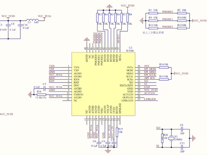
This project focuses on the hardware design of a W5500-based Ethernet network module without MCU integration. By implementing proper power regulation, SPI interface breakout, RJ45 magnetics, and signal routing practices, the design serves as an educational reference for makers and students learning Ethernet schematic and PCB principles.
Hardware Architecture Overview
This module consists of four critical hardware sections:
1️⃣ Power Supply Design
3.3V regulated supply
Multiple decoupling capacitors near each VDD pin
Stable power layout with short return paths
Power integrity is crucial because Ethernet PHY operations are sensitive to voltage noise.
2️⃣ Clock Circuit
25 MHz crystal oscillator
Load capacitors matched to crystal specification
Minimal trace length between crystal and chip
Improper clock routing can cause link instability.
3️⃣ SPI Communication Interface
The module exposes:
MOSI
MISO
SCK
CS
RESET
INT (optional)
This modular SPI design allows the board to connect to:
Arduino
STM32
RP2040
Any SPI-capable controller
The hardware module remains independent of firmware design.
4️⃣ Ethernet PHY & RJ45 Section
Differential TX+/TX- and RX+/RX- routing
Magnetics-integrated RJ45 connector
ESD protection diodes
Controlled impedance PCB traces
Ethernet reliability depends heavily on proper PCB layout practices.
Why This Matters for Makers and Education
Most hobby projects hide Ethernet complexity behind development boards. This module:
Exposes real Ethernet hardware design
Demonstrates signal integrity principles
Teaches power decoupling strategies
Encourages modular hardware thinking
It is an ideal teaching reference for:
Embedded hardware labs
Maker PCB workshops
Networking hardware courses
Industrial Design Perspective
Even though positioned for hobby learning, the design principles align with industrial standards:
Clean power domain separation
Proper impedance routing
EMI/ESD consideration
Hardware modularity
This makes it a strong foundation for transitioning from maker projects to professional hardware development.
FAQ (WIZnet-Focused)
Q1: Why design a standalone W5500 module instead of using a development board?
A: It allows full control over schematic and PCB layout, which is essential for learning real Ethernet hardware design principles.
Q2: What voltage does W5500 require?
A: W5500 operates at 3.3V and requires proper decoupling to ensure stable PHY operation.
Q3: Why is the 25 MHz crystal important?
A: It provides the timing reference for Ethernet communication. Poor clock design can cause unstable links.
Q4: Does this module include an MCU?
A: No. It is designed as a pure Ethernet interface module, connectable to any SPI-capable controller.
Q5: Is this suitable for industrial applications?
A: Yes, if designed with proper PCB layout, ESD protection, and power integrity considerations.
Tags
#W5500 #EthernetModule #HardwareDesign #PCBDesign #EmbeddedEducation #MakerProject
🇰🇷 KOREAN VERSION
W5500 기반 이더넷 네트워크 모듈을 하드웨어 수준에서 설계하는 방법은?
(How to Design a W5500 Ethernet Network Module at the Hardware Level?)
프로젝트 개요 (52단어)
이 프로젝트는 MCU 통합 없이 W5500 기반 이더넷 네트워크 모듈의 하드웨어 설계를 다룹니다. 전원 설계, SPI 인터페이스, RJ45 마그네틱, 신호 라우팅 원칙을 구현하여 메이커와 학생들이 이더넷 회로 및 PCB 설계 원리를 학습할 수 있는 교육용 레퍼런스를 제공합니다.
하드웨어 구조 분석
1. 전원 설계
3.3V 안정적 공급
디커플링 캐패시터 적절 배치
전원 리턴 경로 최소화
2. 클럭 회로
25MHz 크리스탈
짧은 배선
정확한 부하 캐패시턴스
3. SPI 인터페이스
MOSI / MISO / SCK / CS
RESET / INT
MCU와 독립적으로 동작하는 모듈 구조입니다.
4. 이더넷 PHY 회로
차동 신호 라우팅
RJ45 + 마그네틱
ESD 보호
PCB 레이아웃이 통신 안정성을 결정합니다.
교육 및 메이커 관점
이 설계는:
실제 이더넷 회로 구조 이해
신호 무결성 학습
산업용 설계 원칙 습득
에 매우 적합합니다.
FAQ
Q1: 왜 단독 W5500 모듈을 설계하나요?
A: 실제 이더넷 회로 설계 원리를 배우기 위해서입니다.
Q2: 동작 전압은?
A: 3.3V입니다.
Q3: 25MHz 클럭이 중요한 이유는?
A: 이더넷 타이밍 기준이 되기 때문입니다.
Q4: MCU가 포함되나요?
A: 아닙니다. SPI 기반 독립 모듈입니다.
Q5: 산업용으로도 가능합니까?
A: 적절한 PCB 설계 시 가능합니다.