



How to Build a Commercial FPGA Ethernet Architecture with W5500?
This project presents a Verilog-based interface between an FPGA and the WIZnet W5500 Ethernet controller.
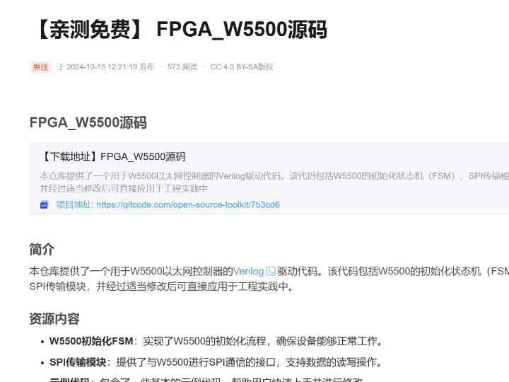
How to Build a Commercial FPGA Ethernet Architecture with W5500?
Summary
This project presents a Verilog-based interface between an FPGA and the WIZnet W5500 Ethernet controller. The published material identifies two principal RTL components: a W5500 initialization finite-state machine and an SPI transfer module. In a commercial FPGA design, the W5500 can provide Ethernet MAC, PHY, hardwired TCP/IP processing, eight socket contexts, and packet buffering, while the FPGA implements deterministic control, data acquisition, framing, and application-specific state machines.
What the Project Does
The source article describes a Verilog driver intended to operate the W5500 directly from FPGA logic. It links to a GitCode repository and states that the project includes:
A W5500 initialization finite-state machine
An SPI read/write transfer module
Basic example code
Verilog sources intended for modification and integration into a larger FPGA project
The linked repository repeats the same limited description and is marked with an MIT license. The public pages reviewed do not expose enough source content to verify individual module names, register constants, top-level ports, supported socket modes, or a complete transmit-and-receive implementation. The article also states that some of its text was AI-assisted, so its architectural claims should be treated as an overview rather than proof of tested RTL behavior.
A complete commercial architecture based on the stated project would use the following data path:
Sensor, converter, motor-control, or application logic → FPGA data buffer → application protocol FSM → W5500 socket-control FSM → SPI controller → W5500 → Ethernet network
The return path would operate in reverse:
Ethernet network → W5500 receive buffer → SPI controller → socket receive FSM → FPGA FIFO or application logic
This arrangement allows the FPGA to concentrate on deterministic data processing while the W5500 handles Ethernet framing, supported TCP/IP protocols, socket state, and internal network buffers.
Where WIZnet Fits
The relevant device is the WIZnet W5500. It integrates a hardwired TCP/IP engine, a 10/100 Ethernet MAC and PHY, eight independent hardware sockets, and 32 KB of internal transmit and receive buffer memory. It communicates with the host through SPI at up to 80 MHz.
In this FPGA architecture, the W5500 operates as a network offload peripheral rather than as a simple Ethernet PHY. The FPGA does not need to implement the complete Ethernet MAC, ARP engine, IPv4 processing, TCP state machine, retransmission behavior, socket buffers, and PHY interface in programmable logic.
The FPGA remains responsible for:
W5500 reset and startup sequencing
SPI transaction generation
Register configuration
Socket command sequencing
Payload movement between FPGA buffers and W5500 memory
Application protocol framing
Timeout and recovery policies
Device-specific control and signal processing
The W5500 is responsible for supported hardware network functions, including TCP, UDP, ICMP, IPv4, ARP, IGMP, and PPPoE. It also contains the Ethernet MAC, PHY, socket state, and packet buffer memory.
For a commercial FPGA product, this partitioning can reduce RTL scope and verification effort. The design team still needs to verify the SPI controller, register sequencing, socket state machines, buffer boundaries, reset recovery, and application behavior under network faults.
Implementation Notes
The available article and repository overview do not expose verifiable Verilog files, file paths, or line-level source code. Therefore, no repository code is quoted here. The following is an architecture-level implementation model derived from the documented presence of an initialization FSM and SPI transfer module, combined with the official W5500 interface requirements.
Top-Level FPGA Architecture
A production-oriented design can be divided into these RTL blocks:
1. Clock and reset controller
This block generates internal reset signals and ensures that the W5500 reset pin remains asserted until the FPGA clock and power rails are stable. It should also provide a controlled reinitialization path after watchdog, SPI, PHY, or socket failures.
2. SPI master
The SPI master generates SCLK, MOSI, MISO sampling, and chip-select timing. It should support variable-length transfers because W5500 transactions contain an address phase, control phase, and one or more data bytes.
Useful interfaces include:
Command valid
Read or write selection
Register address
W5500 block-select value
Transfer length
TX data stream
RX data stream
Busy and completion status
Timeout or fault indication
A commercial implementation should support burst transfers so payload data can move efficiently between FPGA FIFOs and W5500 socket memory.
3. W5500 register-access layer
This block converts logical operations into W5500 SPI frames. It combines the register offset, block-select bits, read/write control, and operating mode into the required SPI command format.
The layer should hide physical SPI details from the initialization and socket state machines. Higher-level logic should request operations such as “write common register,” “read socket status,” or “transfer socket payload” rather than manually constructing every SPI byte.
4. Initialization FSM
The initialization FSM should perform a controlled startup sequence:
Assert and release W5500 reset.
Wait for the required startup interval.
Confirm that stable SPI register access is possible.
Configure socket transmit and receive memory allocation.
Write the MAC address.
Write the IPv4 address, subnet mask, and gateway.
Configure retry timeout and retry count.
Check PHY link status.
Place the application socket into the required mode.
Report initialization complete or fault.
The source material confirms that an initialization FSM exists, but the exact register order and error handling cannot be verified from the public view.
5. Socket-control FSM
Each active socket requires sequencing around the W5500 socket registers and commands. Depending on the product, this block may implement:
TCP client connection
TCP server listen and accept behavior
UDP transmit and receive
Socket close and reopen
Destination address and port configuration
Receive-size checking
Send completion checking
Timeout recovery
The socket controller should not assume that commands complete immediately. It must poll or respond to socket status and interrupt conditions.
6. TX data path
The transmit path can use a FIFO between application logic and the W5500 interface. A typical sequence is:
Application logic writes payload data into a FIFO.
The socket FSM checks available W5500 transmit memory.
The transfer engine reads the current W5500 TX write pointer.
Payload data is written through SPI into socket TX memory.
The write pointer is updated.
The SEND command is issued.
Completion or timeout is checked.
The FPGA must correctly handle circular buffer wraparound when a transfer crosses the end of a W5500 socket buffer.
7. RX data path
A typical receive sequence is:
Read the socket receive-size register.
Read the current RX read pointer.
Transfer available data into an FPGA FIFO.
Handle circular buffer wraparound.
Update the RX read pointer.
Issue the receive-complete command.
Deliver framed data to application logic.
Application framing deserves special attention. TCP delivers a byte stream rather than preserving application message boundaries, so the FPGA must define message length, delimiter, header, or checksum rules.
8. Interrupt and polling controller
The W5500 interrupt output can reduce constant register polling. However, the FPGA should still include timeout counters because a missing interrupt, link transition, or incomplete command must not leave the state machine permanently blocked.
9. Application protocol engine
This block converts FPGA data into the commercial product’s message format. Examples include:
Fixed binary telemetry frames
Command and status packets
Measurement blocks
Modbus TCP application data
Proprietary control protocols
Device discovery messages
The W5500 handles transport functions, but it does not define the application protocol.
10. Diagnostics and watchdog
The architecture should expose counters and status registers for:
SPI timeouts
Socket reconnects
PHY link loss
Receive overflow
Transmit underrun
Invalid message length
Protocol checksum failure
W5500 reinitialization
Watchdog activation
These diagnostics are important for manufacturing tests and field failure analysis.
Direct RTL Versus an FPGA Soft-Core CPU
A soft-core processor architecture places a processor such as AMD MicroBlaze or Intel Nios V inside the FPGA fabric. These processors execute software and can be connected to SPI, memory, timers, interrupts, and other peripherals. AMD describes MicroBlaze as a configurable soft processor for supported FPGAs, while Intel describes Nios V as a RISC-V soft processor implemented with FPGA IP.
A soft-core implementation would typically use this structure:
FPGA application logic → bus or FIFO → soft-core CPU → software W5500 driver → SPI controller → W5500
The direct-RTL project instead implies this structure:
FPGA application logic → hardware FSMs → RTL SPI controller → W5500
Direct RTL provides tighter cycle-level control and avoids processor firmware, instruction memory, data memory, and software scheduling. It can be appropriate for a fixed protocol with limited socket behavior and strict timing requirements.
A soft-core CPU generally makes complex control flow easier to implement. DHCP, DNS, configuration menus, multiple application protocols, firmware updates, diagnostic shells, and changing product requirements are usually simpler to maintain in C or C++ than as large Verilog state machines.
The commercial trade-off is therefore not simply performance. It is primarily a choice between:
Deterministic, specialized RTL with a larger hardware-verification burden
Software flexibility with additional FPGA resource, memory, toolchain, and firmware-validation requirements
A hybrid design is also possible. Time-critical data movement can remain in RTL, while a soft-core CPU performs configuration, network management, and maintenance functions.
Practical Tips / Pitfalls
Validate W5500 register reads before implementing socket traffic. A stable register test is the foundation for all higher-level debugging.
Use burst SPI transfers for payload movement. Byte-by-byte controller handshakes can limit throughput even when the SPI clock is high.
Handle W5500 TX and RX circular-buffer wraparound explicitly. This is a common failure point in custom hardware interfaces.
Add a timeout to every FSM state that waits for SPI completion, link status, socket state, send completion, or received data.
Synchronize the W5500 interrupt input before using it inside FPGA logic, and protect clock-domain crossings between network control and application datapaths.
Reserve socket and buffer resources during architecture design. The W5500 provides eight sockets and a shared 32 KB memory pool, so allocation is finite.
Separate transport recovery from full-system reset. Close or reopen a failed socket first, reinitialize the W5500 when necessary, and reset the complete FPGA system only as a final recovery action.
FAQ
Q: Why use the W5500 with an FPGA in a commercial product?
The W5500 removes the need to implement a complete Ethernet MAC, PHY interface, supported TCP/IP protocols, socket state, retransmission logic, and packet memory in FPGA logic. This reduces the custom networking RTL that must be designed and verified while preserving an FPGA-controlled hardware datapath.
Q: How does the W5500 connect to the FPGA?
It connects through SPI using SCLK, MOSI, MISO, and chip select. A practical design also connects hardware reset and usually the interrupt output. The FPGA must generate the W5500 address, control, and data phases and must support both register and socket-buffer transfers.
Q: What role does the W5500 play in this project?
It acts as the Ethernet and hardwired TCP/IP endpoint. The FPGA initialization FSM configures it, the SPI module transfers commands and payloads, and additional socket-control logic is required to establish connections and move data between W5500 memory and the FPGA application.
Q: Can beginners implement the complete architecture?
The basic SPI module is approachable for a developer familiar with Verilog state machines. A complete commercial implementation is more difficult because it requires socket-state handling, circular-buffer management, asynchronous input synchronization, timeout recovery, application framing, simulation, and hardware-level Ethernet validation.
Q: How does direct FPGA RTL compare with using a soft-core CPU?
Direct RTL can provide deterministic behavior and lower software dependence, but complex network control becomes a hardware-verification problem. A soft-core CPU consumes FPGA logic and memory but makes DHCP, diagnostics, configuration, protocol changes, and maintenance features easier to implement in software. Fixed-function products may favor RTL, while feature-rich or frequently changing products often benefit from a soft-core or hybrid architecture.
Source
Original article: CSDN, FPGA_W5500 Source Code. The article was published under CC BY-SA 4.0 and states that some content was AI-assisted.
Linked repository: GitCode, open-source-toolkit/7b3cd6. The repository describes a Verilog W5500 driver containing an initialization FSM, SPI transfer module, and examples. It is marked as MIT-licensed.
Technical reference: WIZnet W5500 official documentation and datasheet.
Comparison references: AMD MicroBlaze and Intel Nios V official processor documentation.
Tags
#W5500 #WIZnet #FPGA #Verilog #SPI #Ethernet #HardwareTCPIP #RTL #SoftCoreCPU #MicroBlaze #NiosV #CommercialEmbedded
W5500으로 상용 FPGA 이더넷 아키텍처를 어떻게 구축할 수 있을까?
요약
이 프로젝트는 FPGA와 WIZnet W5500 이더넷 컨트롤러를 연결하기 위한 Verilog 기반 인터페이스를 다룹니다. 공개된 자료에서는 W5500 초기화 유한상태기계와 SPI 전송 모듈을 주요 RTL 구성 요소로 설명합니다. 상용 FPGA 설계에서 W5500은 이더넷 MAC, PHY, 하드와이어드 TCP/IP 처리, 8개 소켓, 패킷 버퍼를 담당하고, FPGA는 결정론적 제어, 데이터 수집, 프레이밍, 애플리케이션별 상태 머신을 구현할 수 있습니다.
프로젝트가 하는 일
원문에서는 FPGA 로직이 W5500을 직접 제어할 수 있도록 설계된 Verilog 드라이버를 소개합니다. 연결된 GitCode 저장소에는 다음 구성 요소가 포함된 것으로 설명되어 있습니다.
W5500 초기화 유한상태기계
SPI 읽기 및 쓰기 전송 모듈
기본 예제 코드
상위 FPGA 프로젝트에 수정 및 통합할 수 있는 Verilog 소스
연결된 저장소도 동일한 범위의 설명을 제공하며 MIT 라이선스로 표시되어 있습니다. 다만 검토 가능한 공개 화면만으로는 개별 모듈 이름, 레지스터 상수, 최상위 포트, 지원되는 소켓 모드, 전체 송수신 구현을 확인하기 어렵습니다.
원문에는 일부 내용이 AI의 도움을 받아 작성되었다는 고지도 있으므로, 아키텍처 설명은 개요로 활용하고 실제 RTL 동작은 저장소 소스와 하드웨어 시험을 통해 검증해야 합니다.
완성된 상용 아키텍처의 데이터 흐름은 다음과 같이 구성할 수 있습니다.
센서, 변환기, 모터 제어 또는 애플리케이션 로직 → FPGA 데이터 버퍼 → 애플리케이션 프로토콜 FSM → W5500 소켓 제어 FSM → SPI 컨트롤러 → W5500 → 이더넷 네트워크
수신 경로는 반대로 동작합니다.
이더넷 네트워크 → W5500 수신 버퍼 → SPI 컨트롤러 → 소켓 수신 FSM → FPGA FIFO 또는 애플리케이션 로직
이 구조에서는 FPGA가 결정론적인 데이터 처리에 집중하고, W5500이 이더넷 프레임, 지원되는 TCP/IP 프로토콜, 소켓 상태, 내부 네트워크 버퍼를 처리합니다.
WIZnet이 적용되는 위치
사용되는 제품은 WIZnet W5500입니다. W5500은 하드와이어드 TCP/IP 엔진, 10/100 이더넷 MAC과 PHY, 8개의 독립적인 하드웨어 소켓, 32 KB의 내부 송수신 버퍼를 통합합니다. 호스트와는 최대 80 MHz SPI를 통해 통신합니다.
이 FPGA 아키텍처에서 W5500은 단순한 이더넷 PHY가 아니라 네트워크 오프로드 주변장치로 동작합니다. FPGA에서 이더넷 MAC, ARP 엔진, IPv4 처리, TCP 상태 머신, 재전송 처리, 소켓 버퍼, PHY 인터페이스 전체를 직접 구현할 필요가 없습니다.
FPGA가 담당하는 기능은 다음과 같습니다.
W5500 리셋 및 시작 시퀀스
SPI 트랜잭션 생성
레지스터 설정
소켓 명령 시퀀스
FPGA 버퍼와 W5500 메모리 사이의 페이로드 이동
애플리케이션 프로토콜 프레이밍
타임아웃 및 장애 복구 정책
제품별 제어 및 신호 처리
W5500은 TCP, UDP, ICMP, IPv4, ARP, IGMP, PPPoE 등 지원되는 하드웨어 네트워크 기능을 담당합니다. 이더넷 MAC, PHY, 소켓 상태, 패킷 버퍼 메모리도 포함합니다.
상용 FPGA 제품에서는 이러한 역할 분담을 통해 RTL 구현 범위와 검증 부담을 줄일 수 있습니다. 그러나 SPI 컨트롤러, 레지스터 시퀀스, 소켓 상태 머신, 버퍼 경계, 리셋 복구, 네트워크 장애 상황의 애플리케이션 동작은 별도로 검증해야 합니다.
구현 참고 사항
공개된 원문과 저장소 개요에서는 검증 가능한 Verilog 파일, 파일 경로, 코드 라인을 확인할 수 없습니다. 따라서 실제 저장소 코드는 인용하지 않습니다. 아래 내용은 공개 자료에서 언급된 초기화 FSM과 SPI 전송 모듈, 그리고 W5500의 공식 인터페이스 요구사항을 기반으로 정리한 아키텍처 수준의 구현 모델입니다.
최상위 FPGA 아키텍처
양산을 고려한 설계는 다음 RTL 블록으로 구분할 수 있습니다.
1. 클럭 및 리셋 컨트롤러
이 블록은 내부 리셋 신호를 생성하고 FPGA 클럭과 전원 레일이 안정될 때까지 W5500 리셋 핀을 활성 상태로 유지합니다.
watchdog 오류, SPI 오류, PHY 링크 오류, 소켓 장애가 발생했을 때 W5500만 제어된 방식으로 재초기화할 수 있는 경로도 제공해야 합니다.
2. SPI 마스터
SPI 마스터는 SCLK, MOSI, MISO 샘플링, 칩 선택 타이밍을 생성합니다. W5500 트랜잭션은 주소 단계, 제어 단계, 하나 이상의 데이터 바이트로 구성되므로 가변 길이 전송을 지원해야 합니다.
유용한 인터페이스 신호는 다음과 같습니다.
명령 유효 신호
읽기 또는 쓰기 선택
레지스터 주소
W5500 블록 선택 값
전송 길이
TX 데이터 스트림
RX 데이터 스트림
동작 중 및 완료 상태
타임아웃 또는 오류 표시
상용 구현에서는 FPGA FIFO와 W5500 소켓 메모리 사이에서 데이터를 효율적으로 이동할 수 있도록 버스트 전송을 지원해야 합니다.
3. W5500 레지스터 접근 계층
이 블록은 논리적 레지스터 명령을 W5500 SPI 프레임으로 변환합니다. 레지스터 오프셋, 블록 선택 비트, 읽기 또는 쓰기 제어, 동작 모드를 조합하여 SPI 명령을 생성합니다.
초기화 및 소켓 FSM이 물리적인 SPI 형식을 직접 다루지 않도록 해야 합니다. 상위 로직은 각 SPI 바이트를 직접 구성하는 대신 다음과 같은 논리 연산을 요청하는 형태가 적절합니다.
공통 레지스터 쓰기
소켓 상태 읽기
소켓 TX 메모리에 데이터 쓰기
소켓 RX 메모리에서 데이터 읽기
4. 초기화 FSM
초기화 FSM은 다음 순서로 제어된 시작 절차를 수행할 수 있습니다.
W5500 리셋을 활성화하고 해제합니다.
필요한 시작 대기 시간을 적용합니다.
SPI 레지스터 접근이 안정적인지 확인합니다.
소켓별 송수신 메모리를 할당합니다.
MAC 주소를 설정합니다.
IPv4 주소, 서브넷 마스크, 게이트웨이를 설정합니다.
재전송 타임아웃과 재시도 횟수를 설정합니다.
PHY 링크 상태를 확인합니다.
애플리케이션 소켓을 필요한 모드로 설정합니다.
초기화 완료 또는 오류 상태를 출력합니다.
공개 자료에서는 초기화 FSM이 존재한다고 설명하지만, 실제 레지스터 설정 순서와 오류 처리는 검증할 수 없습니다.
5. 소켓 제어 FSM
각 활성 소켓은 W5500 소켓 레지스터와 명령을 순서대로 처리해야 합니다. 제품 요구사항에 따라 다음 기능을 구현할 수 있습니다.
TCP 클라이언트 연결
TCP 서버 대기 및 연결 수락
UDP 송수신
소켓 닫기 및 재개방
목적지 IP 주소와 포트 설정
수신 데이터 크기 확인
전송 완료 확인
타임아웃 복구
W5500 명령이 즉시 완료된다고 가정해서는 안 됩니다. 소켓 상태 레지스터나 인터럽트 상태를 확인하여 명령 완료 여부를 판단해야 합니다.
6. TX 데이터 경로
송신 경로는 애플리케이션 로직과 W5500 인터페이스 사이에 FIFO를 배치할 수 있습니다.
일반적인 송신 순서는 다음과 같습니다.
애플리케이션 로직이 페이로드를 FIFO에 기록합니다.
소켓 FSM이 W5500의 사용 가능한 TX 메모리를 확인합니다.
현재 TX 쓰기 포인터를 읽습니다.
SPI를 통해 소켓 TX 메모리에 페이로드를 기록합니다.
TX 쓰기 포인터를 갱신합니다.
SEND 명령을 실행합니다.
전송 완료 또는 타임아웃을 확인합니다.
전송 데이터가 소켓 버퍼 끝을 넘어가면 원형 버퍼 시작 위치로 이어서 기록해야 합니다. 이 래핑 처리는 FPGA 로직에서 명시적으로 구현해야 합니다.
7. RX 데이터 경로
일반적인 수신 순서는 다음과 같습니다.
소켓의 수신 데이터 크기를 읽습니다.
현재 RX 읽기 포인터를 읽습니다.
사용 가능한 데이터를 FPGA FIFO로 전송합니다.
원형 버퍼 래핑을 처리합니다.
RX 읽기 포인터를 갱신합니다.
수신 완료 명령을 실행합니다.
프레임 단위 데이터를 애플리케이션 로직으로 전달합니다.
애플리케이션 프레이밍은 별도로 설계해야 합니다. TCP는 메시지 단위가 아니라 바이트 스트림을 제공하므로, FPGA 프로토콜에는 길이 필드, 구분자, 헤더, 체크섬과 같은 메시지 경계 규칙이 필요합니다.
8. 인터럽트 및 폴링 컨트롤러
W5500 인터럽트 출력을 사용하면 지속적인 레지스터 폴링을 줄일 수 있습니다. 그러나 인터럽트 누락, 링크 변화, 완료되지 않은 명령 때문에 FSM이 영구적으로 대기하지 않도록 모든 주요 상태에 타임아웃 카운터를 적용해야 합니다.
비동기 인터럽트 입력은 FPGA 클럭 도메인에 맞게 동기화한 후 사용해야 합니다.
9. 애플리케이션 프로토콜 엔진
이 블록은 FPGA 데이터를 상용 제품의 메시지 형식으로 변환합니다.
예시는 다음과 같습니다.
고정 길이 바이너리 텔레메트리 프레임
명령 및 상태 패킷
측정 데이터 블록
Modbus TCP 애플리케이션 데이터
독자적인 제어 프로토콜
장치 검색 메시지
W5500은 전송 계층을 처리하지만 애플리케이션 프로토콜 자체를 정의하지는 않습니다.
10. 진단 및 watchdog
다음 항목을 위한 상태 레지스터와 카운터를 제공하는 것이 좋습니다.
SPI 타임아웃 횟수
소켓 재연결 횟수
PHY 링크 손실 횟수
수신 FIFO 오버플로
송신 언더런
잘못된 메시지 길이
프로토콜 체크섬 오류
W5500 재초기화 횟수
watchdog 동작 횟수
이러한 진단 정보는 생산 시험과 현장 장애 분석에 중요합니다.
직접 RTL 구현과 FPGA 소프트 코어 CPU 비교
소프트 코어 프로세서 아키텍처에서는 AMD MicroBlaze나 Intel Nios V와 같은 프로세서를 FPGA 패브릭 내부에 구현합니다. 이 프로세서는 소프트웨어를 실행하며 SPI, 메모리, 타이머, 인터럽트 등의 주변장치와 연결됩니다.
소프트 코어 구조는 일반적으로 다음과 같습니다.
FPGA 애플리케이션 로직 → 버스 또는 FIFO → 소프트 코어 CPU → 소프트웨어 W5500 드라이버 → SPI 컨트롤러 → W5500
직접 RTL 방식은 다음과 같은 구조입니다.
FPGA 애플리케이션 로직 → 하드웨어 FSM → RTL SPI 컨트롤러 → W5500
직접 RTL 구현은 사이클 단위의 제어가 가능하며 프로세서 펌웨어, 명령 메모리, 데이터 메모리, 소프트웨어 스케줄링이 필요하지 않습니다. 소켓 동작이 단순하고 프로토콜이 고정되어 있으며 엄격한 타이밍이 필요한 제품에 적합할 수 있습니다.
반면 소프트 코어 CPU는 복잡한 제어 흐름을 구현하기 쉽습니다. DHCP, DNS, 설정 메뉴, 여러 애플리케이션 프로토콜, 펌웨어 업데이트, 진단 셸, 변경되는 제품 요구사항은 대규모 Verilog FSM보다 C 또는 C++로 구현하고 유지보수하기가 일반적으로 쉽습니다.
상용 제품에서의 핵심 차이는 단순한 성능이 아닙니다.
직접 RTL은 결정론적이고 특화된 동작을 제공하지만 하드웨어 검증 부담이 큽니다.
소프트 코어는 FPGA 논리와 메모리를 추가로 사용하지만 소프트웨어 변경과 유지보수가 쉽습니다.
혼합형 구조도 가능합니다. 시간에 민감한 데이터 이동은 RTL이 처리하고, 소프트 코어 CPU는 설정, 네트워크 관리, 진단, 유지보수 기능을 담당할 수 있습니다.
실무 팁과 주의사항
소켓 통신을 구현하기 전에 W5500 레지스터 읽기부터 검증해야 합니다. 안정적인 레지스터 접근은 모든 상위 디버깅의 기반입니다.
페이로드 전송에는 버스트 SPI를 사용해야 합니다. 바이트마다 제어 핸드셰이크를 수행하면 높은 SPI 클럭을 사용해도 실제 처리량이 제한될 수 있습니다.
W5500 TX 및 RX 원형 버퍼의 래핑을 명시적으로 처리해야 합니다. 커스텀 하드웨어 인터페이스에서 자주 발생하는 오류 지점입니다.
SPI 완료, 링크 상태, 소켓 상태, SEND 완료, 데이터 수신을 기다리는 모든 FSM 상태에 타임아웃을 추가해야 합니다.
W5500 인터럽트 입력은 FPGA 내부에서 사용하기 전에 동기화해야 하며, 네트워크 제어 블록과 애플리케이션 데이터 경로가 다른 클럭을 사용한다면 클럭 도메인 교차를 별도로 처리해야 합니다.
아키텍처 설계 단계에서 소켓과 버퍼를 미리 배정해야 합니다. W5500은 8개 소켓과 공유 32 KB 메모리라는 고정된 자원을 제공합니다.
전송 계층 복구와 전체 시스템 리셋을 분리해야 합니다. 먼저 실패한 소켓을 닫고 다시 열고, 필요한 경우 W5500만 재초기화하며, 전체 FPGA 시스템 리셋은 마지막 수단으로 사용해야 합니다.
FAQ
Q: 상용 FPGA 제품에서 W5500을 사용하는 이유는 무엇인가요?
W5500을 사용하면 이더넷 MAC, PHY 인터페이스, 지원되는 TCP/IP 프로토콜, 소켓 상태, 재전송 로직, 패킷 메모리를 FPGA에서 직접 구현할 필요가 없습니다. 따라서 네트워크 관련 커스텀 RTL의 범위와 검증 부담을 줄이면서 FPGA가 제어하는 하드웨어 데이터 경로를 유지할 수 있습니다.
Q: W5500은 FPGA와 어떻게 연결하나요?
SCLK, MOSI, MISO, 칩 선택 신호로 구성된 SPI 인터페이스를 사용합니다. 실무 설계에서는 하드웨어 리셋과 인터럽트 출력도 연결하는 것이 일반적입니다. FPGA는 W5500의 주소 단계, 제어 단계, 데이터 단계를 생성하고 레지스터와 소켓 버퍼 전송을 모두 지원해야 합니다.
Q: 이 프로젝트에서 W5500은 어떤 역할을 하나요?
W5500은 이더넷 및 하드와이어드 TCP/IP 엔드포인트 역할을 합니다. FPGA 초기화 FSM이 W5500을 설정하고, SPI 모듈이 명령과 페이로드를 전송합니다. 실제 연결 수립과 데이터 이동에는 추가적인 소켓 제어 로직이 필요합니다.
Q: 초보자도 전체 아키텍처를 구현할 수 있나요?
기본 SPI 모듈은 Verilog 상태 머신에 익숙한 개발자라면 접근할 수 있습니다. 그러나 완성된 상용 구현에는 소켓 상태 처리, 원형 버퍼 관리, 비동기 입력 동기화, 타임아웃 복구, 애플리케이션 프레이밍, 시뮬레이션, 실제 이더넷 하드웨어 검증이 필요하므로 난이도가 높습니다.
Q: 직접 FPGA RTL로 구현하는 방식은 소프트 코어 CPU와 어떻게 다른가요?
직접 RTL은 결정론적인 동작과 낮은 소프트웨어 의존성을 제공하지만 복잡한 네트워크 제어가 하드웨어 검증 문제로 바뀝니다. 소프트 코어 CPU는 FPGA 논리와 메모리를 사용하지만 DHCP, 진단, 설정, 프로토콜 변경, 유지보수 기능을 소프트웨어로 구현하기 쉽습니다. 고정 기능 제품은 RTL이 적합할 수 있고, 기능이 많거나 변경이 잦은 제품은 소프트 코어 또는 혼합형 아키텍처가 유리할 수 있습니다.
출처
원문: CSDN, FPGA_W5500 소스 코드 소개
https://blog.csdn.net/gitblog_09811/article/details/142944641
원문은 CC BY-SA 4.0 라이선스로 게시되었으며 일부 내용이 AI의 도움을 받아 작성되었다고 명시합니다.
연결된 저장소: GitCode, open-source-toolkit/7b3cd6
https://gitcode.com/open-source-toolkit/7b3cd6
저장소에서는 초기화 FSM, SPI 전송 모듈, 예제를 포함하는 Verilog W5500 드라이버로 소개하고 있으며 MIT 라이선스로 표시되어 있습니다.
기술 참고 자료: WIZnet W5500 공식 문서 및 데이터시트
https://docs.wiznet.io/Product/Chip/Ethernet/W5500
비교 참고 자료: AMD MicroBlaze 및 Intel Nios V 공식 프로세서 문서
태그
#W5500 #WIZnet #FPGA #Verilog #SPI #Ethernet #HardwareTCPIP #RTL #SoftCoreCPU #MicroBlaze #NiosV #CommercialEmbedded