


How Does a Reconfigurable Multi-Channel Data Acquisition Patent Use WIZnet W5500?
A patent from Southwest Univ. of Science & Technology reconfigures two ADCs for multi-channel or high-rate sampling, streaming data over Ethernet via W5500.
WIZnet - W5500
x 1

📌 Overview
CN111342841B is a granted Chinese invention patent for a reconfigurable multi-channel signal acquisition and transmission system. It was filed on 2020-03-10 by Southwest University of Science and Technology, published on 2020-06-26, and granted on 2023-02-28, with inventors Wu Chun, Yang Dongxu, Jiang Hong, Zeng Min, Yi Zhiqiang, and Liu Xiong.
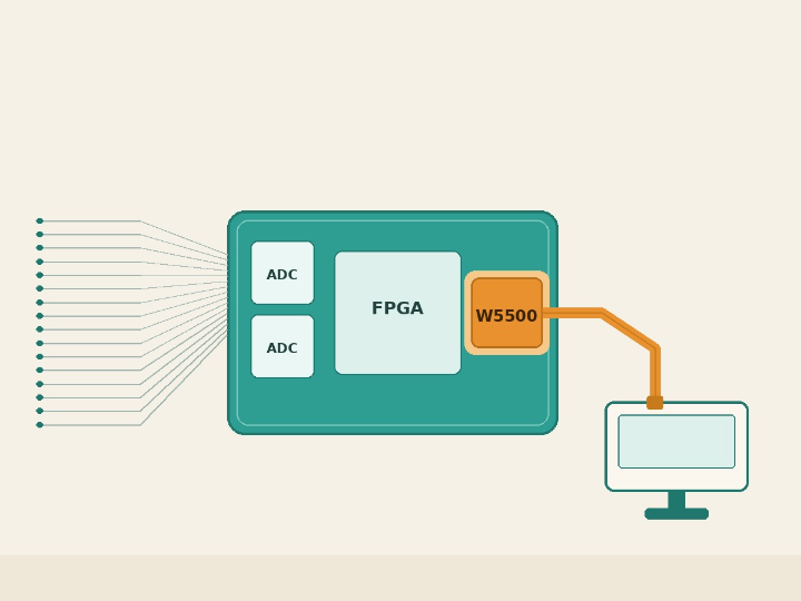
The patent tackles a familiar problem in data acquisition hardware: a board can offer many input channels or a fast sampling rate, but getting both usually means adding more ADC chips, which raises cost. The disclosed answer is a Xilinx Kintex-7 FPGA that dynamically reroutes two 16-bit ADCs between two operating modes, so a fixed two-ADC board can act as either a 16-channel synchronous recorder or an 8-channel high-rate recorder. A WIZnet W5500 then carries the acquired data back to a host computer over Ethernet, while the FPGA stays focused on acquisition and timing rather than on running a network stack.
The reconfigurable ADC path is the headline invention, but the W5500 is the system's whole road off the board: it turns the FPGA's internal data FIFO into TCP/IP traffic on an ordinary Ethernet cable.
Key Context: Channels vs Sampling Rate, and Hardwired TCP/IP
Two ideas make the rest of the article readable.
First, the channel-count versus sampling-rate tradeoff. In a conventional design, each analog input needs converter capacity. To sample faster you can make several ADCs take turns on the same input (interleaving), but then those converters are no longer free to serve their own channels, so the usable channel count drops. To keep all channels you give each one steady converter time, which caps the rate. The patent's point is that you should be able to pick either behavior on the same hardware, at no extra ADC cost.
Second, hardwired TCP/IP offload. The WIZnet W5500 contains the TCP/IP stack in silicon. The host controller writes payload bytes into the chip and reads received bytes back over SPI, and the W5500 handles the socket, sequencing, and Ethernet framing itself. In this patent that matters because the main controller is an FPGA, not a CPU running an operating system, so not needing a software TCP/IP stack keeps the FPGA logic simple and deterministic.
System Configuration
The design separates a data acquisition end from a main control end, which the patent notes shortens the analog cable runs and improves noise immunity.
On the acquisition end, sixteen input channels each pass through a two-stage programmable-gain amplifier (an AD8253ARMZ first stage with 1/10/100/1000x gains, then an AD8250ARMZ second stage with 1/2/5/10x gains) and a switchable second-order active low-pass filter. Eight CMOS 2:1 analog multiplexers steer the conditioned signals, and two LTC2358-16 converters (16-bit, eight channels each) perform the actual digitization. A Xilinx Spartan-3 (XC3S400AN) FPGA handles the acquisition-side control and phase logic, with a small FIFO per endpoint.
On the main control end, a Xilinx Kintex-7 (XC7K325T) FPGA gathers data from up to eight acquisition endpoints over SPI, buffers it, writes it to a Samsung eMMC (KLMAG1JETD) for fault tolerance, and hands it to the WIZnet W5500 Ethernet controller, which connects to the RJ-45 jack through an H1102NL isolation transformer. Because each host can concentrate up to eight endpoints, the architecture scales to 128 channels behind a single Ethernet connection.
System Architecture and Data Flow
The flow runs sensor to conditioning to channel-control multiplexers to the two ADCs, then into the acquisition FPGA's FIFO. The acquisition FPGA sends framed samples over SPI to the Kintex-7 main controller. There the data splits two ways: a copy is written to the eMMC as a local, fault-tolerant store, and the live stream is pushed to the W5500. The patent describes this handoff directly: the data-transmission control module writes the contents of an internal TCP_TX_FIFO into the W5500 send buffer over SPI, and simultaneously reads the W5500 receive buffer back into a TCP_RX_FIFO. The W5500 then presents that traffic as TCP/IP on the wire, through the H1102NL transformer to the host.
Two Acquisition Modes on the Same Board
The FPGA's phase-adjustment unit is what makes the board reconfigurable. In full-channel synchronous mode, channels 1 to 8 map to the first LTC2358-16 and channels 9 to 16 to the second, with the two ADC convert clocks (CNV1 and CNV2) aligned so all sixteen channels sample together at a lower rate. In high-rate interleaved mode, both ADCs work on the same eight channels with their convert clocks offset by 180 degrees, so the effective sampling rate doubles while channels 9 to 16 are disabled. Switching modes is a matter of the FPGA reconfiguring the multiplexers and the ADC clock phase, not changing the hardware.
⚙️ Role of the WIZnet W5500
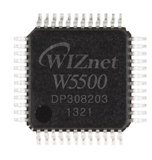
The W5500 is the system's network boundary. The patent states that "the Ethernet transmission chip W5500 is connected to the main control module through a set of SPI interfaces," and that it reaches the physical network through the RXN/RXP and TXN/TXP transceiver pairs and the H1102NL transformer. On the digital side, the Kintex-7 FPGA is the SPI master and the W5500 is the slave.
Its value here is specific. By holding the TCP/IP stack in hardware, the W5500 lets the FPGA move data with simple SPI FIFO reads and writes instead of implementing sockets, retransmission, and Ethernet framing in logic. For a design whose whole purpose is precise, phase-locked analog timing across many channels, keeping the network path as a self-contained, deterministic SPI peripheral is a clean division of labor.
Not a bottleneck, but a boundary: the W5500 absorbs the entire TCP/IP job so the FPGA can spend its resources on ADC clocking, channel routing, and buffering.
Where It Fits: Value and Limits
As an architecture reference, this is a useful pattern for anyone building instrumentation on an FPGA that needs wired data backhaul: multi-sensor vibration and acceleration test benches, distributed industrial acquisition, and any bench setup where a single Ethernet drop should carry many synchronized channels. The reconfiguration idea (reusing two converters for either width or speed) and the eMMC-plus-Ethernet pairing (a local fault-tolerant copy alongside live streaming) are both reusable.
Two honest limits. This is a patent disclosure, not a product or a build guide: it does not publish firmware, PCB files, a BOM, or measured throughput and sampling-rate numbers, so treat the components and modes as the invention's described architecture rather than a benchmarked spec. And its legal status is expired (fee related) as of 2025, which does not change its technical value as a reference but does mean it is no longer an enforceable, maintained patent.
Related WIZnet Maker Projects
Readers interested in the FPGA side can compare this with How to Build FPGA Ethernet with WIZnet W5500 on Verilog?, which drives the W5500 directly from FPGA logic without an MCU driver, the same controller-to-W5500 relationship this patent uses. For the data-acquisition angle, an Ethernet-Based Data Acquisition System for a Cosmic Muon Veto Detector shows W5500 backhaul in a real physics instrument. And for a non-FPGA take on the same SPI-Ethernet interface, Design and Implementation of an Ethernet Interface Based on F28335 and W5500 pairs the W5500 with a TI DSP.
❓ FAQ
Q. What does this patent use the WIZnet W5500 for? It uses the W5500 as the system's Ethernet controller: the main-control Kintex-7 FPGA writes acquired data into the W5500 send buffer over SPI, and the W5500 handles TCP/IP and Ethernet framing to stream that data to a host computer.
Q. How is the W5500 connected in the design? The W5500 sits on the FPGA's SPI bus as a slave and reaches the RJ-45 jack through its RXN/RXP and TXN/TXP pairs and an H1102NL isolation transformer, so the FPGA does not need a software network stack.
Q. What makes the acquisition system "reconfigurable"? An FPGA phase-adjustment unit reroutes two LTC2358-16 ADCs and their convert-clock phases, so the same board runs either as a 16-channel synchronous recorder or an 8-channel recorder at roughly double the sampling rate.
Q. Is this a product I can buy or build from the patent? No. It is a published invention patent (a technical disclosure), not a product or a step-by-step build. It does not include firmware, PCB files, a BOM, or measured performance numbers.
Q. Who holds the patent and what is its status? It was filed by Southwest University of Science and Technology in China and granted in February 2023 (CN111342841B). Its legal status is now expired (fee related) as of 2025, so it is best treated as an architecture reference.