



How to Build FPGA Ethernet with WIZnet W5500 on Verilog?
his project uses an FPGA programmed in Verilog to control a WIZnet W5500 Ethernet controller without relying on an MCU-based C driver.
How to Build FPGA Ethernet with WIZnet W5500 on Verilog?
Summary
This project uses an FPGA programmed in Verilog to control a WIZnet W5500 Ethernet controller without relying on an MCU-based C driver. The FPGA implements the SPI transaction engine, initialization sequence, register controller, socket state machines, transmit path, receive path, and interrupt handling. W5500 provides the 10/100 Ethernet MAC/PHY, hardwired TCP/IP stack, eight hardware sockets, and internal packet memory. This division supports educational experiments, maker prototypes, robotic controllers, industrial data acquisition, and commercial products that require wired networking with explicit hardware timing. The visible GitCode repository confirms the Verilog-based W5500 driver and an MIT license, but it does not expose inspectable HDL files, so project-specific code and performance figures cannot be verified.
What the Project Does
The project replaces a conventional software W5500 driver with FPGA logic. Instead of firmware calling SPI functions sequentially, Verilog finite-state machines generate the W5500 address, control, and data phases directly. The related project overview describes separate initialization, transmit, receive, and interrupt-processing functions, although the actual module boundaries and signal names cannot be confirmed from the visible repository.
A practical system data path is:
Sensor, ADC, encoder, camera interface, or control logic → FPGA processing pipeline → packet FIFO → W5500 socket controller → SPI master → W5500 → transformer and RJ45 → Ethernet network
The receive path operates in reverse:
Ethernet packet → W5500 Rx buffer → SPI read engine → FPGA receive FIFO → parser, control state machine, processor core, or hardware accelerator
This architecture can be adapted to several use cases:
Industrial IoT: deterministic acquisition, machine monitoring, protocol gateways, and wired telemetry.
Robotics: command reception, status reporting, sensor streaming, and communication between fixed robotic cells.
Education: SPI timing, register maps, finite-state machines, socket control, and Ethernet debugging.
Maker: FPGA-based UDP instruments, remote I/O, logic-analyzer streaming, and network-controlled hardware.
Commercial: products requiring controlled startup, fault recovery, measurable latency, and a stable wired interface.
The source states that the driver is written in Verilog and has been applied in multiple projects, but it provides no reproducible benchmark data, FPGA family, resource utilization, clock configuration, or test procedure. Performance should therefore be established on the target board rather than inferred from the project description.
Where WIZnet Fits
The exact WIZnet product is W5500. It sits between the FPGA logic and the Ethernet physical network.
W5500 integrates a hardwired TCP/IP stack, a 10/100 Ethernet MAC and PHY, eight independent sockets, and 32 KB of internal Tx/Rx memory. It supports TCP, UDP, ICMP, IPv4, ARP, IGMP, and PPPoE, and its host interface supports SPI modes 0 and 3 at frequencies up to 80 MHz.
The architectural responsibility is divided as follows:
FPGA logic
Generates SPI clock, chip-select, MOSI, and transaction timing.
Configures common and socket registers.
Allocates W5500 Tx/Rx buffer memory.
Controls socket opening, connection, listening, sending, receiving, and closing.
Moves payloads between FPGA FIFOs and W5500 memory.
Detects timeout, disconnect, receive, and send-complete events.
Applies product-specific packet framing and application logic.
W5500
Terminates the 10/100 Ethernet link.
Handles ARP and IPv4 processing.
Executes hardware TCP and UDP socket functions.
Maintains socket states and retransmission behavior.
Buffers Ethernet payloads independently of FPGA block RAM.
Reports link, socket, and interrupt status through registers.
The W5500 does not replace the FPGA application protocol. It provides transport and socket offload. Protocols such as Modbus/TCP framing, proprietary robot commands, telemetry encoding, or binary measurement formats still need to be implemented in FPGA logic or an embedded processor core.
Implementation Notes
The visible GitCode repository provides only a project description and does not expose the Verilog implementation for inspection. The following structure is therefore an architecture-level integration plan rather than a representation of the unavailable project code.
FPGA and W5500 hardware interface
The FPGA should provide:
SCLK for the W5500 SPI clock
MOSI for FPGA-to-W5500 data
MISO for W5500-to-FPGA data
SCSn for transaction selection
RSTn for hardware recovery
INTn for socket and network events
W5500 operates from 3.3 V and supports SPI modes 0 and 3. The Ethernet side requires the recommended transformer or integrated-magnetics RJ45 circuit, termination components, power filtering, and PCB layout. WIZnet publishes reference schematics for both external-transformer and integrated-RJ45 implementations.
Signals crossing between unrelated clock domains should pass through synchronizers or asynchronous FIFOs. In particular, INTn is asynchronous to the FPGA system clock, and payload producers such as ADC, camera, or motor-control logic may operate in different clock domains from the SPI engine.
SPI transaction engine
A W5500 SPI transaction contains an address phase, a control phase, and a data phase. The control byte selects the register or buffer block, read or write direction, and transfer mode. An FPGA implementation normally uses a finite-state machine that:
Asserts chip select.
Shifts the 16-bit address.
Sends the control byte.
Transfers one or more data bytes.
Deasserts chip select.
Raises a completion or error flag.
The SPI controller should support burst transfers. Reasserting chip select for every payload byte wastes bus cycles and limits throughput. The design should also provide a timeout so that a stalled state machine cannot lock the networking pipeline.
Register initialization
The initialization state machine should first perform a W5500 reset and read VERSIONR; WIZnet defines the W5500 version value as 0x04. It should then configure network identity through GAR, SUBR, SHAR, and SIPR, and verify Ethernet status through PHYCFGR.
Per-socket control uses registers including:
Sn_MR for TCP, UDP, or MACRAW mode
Sn_CR for OPEN, LISTEN, CONNECT, CLOSE, SEND, and RECV
Sn_SR for the current socket state
Sn_IR for connection, receive, disconnect, timeout, and send-complete events
Sn_PORT, Sn_DIPR, and Sn_DPORT for endpoint configuration
Sn_TX_FSR and Sn_RX_RSR for available Tx space and received data
Sn_TX_WR and Sn_RX_RD for buffer-pointer management
These registers are defined in WIZnet’s official W5500 driver header and should be represented in the FPGA as constants or a register-address package rather than repeated numeric literals.
Transmit and receive architecture
The transmit controller should not write a payload until Sn_TX_FSR confirms that enough W5500 buffer space is available. It then writes the payload into the selected socket’s Tx buffer, updates Sn_TX_WR, issues SEND, and waits for SEND_OK or TIMEOUT.
The receive controller should read Sn_RX_RSR, copy the available bytes into an FPGA FIFO, update Sn_RX_RD, and issue RECV. Pointer wraparound must be handled correctly because W5500 buffer pointers are circular. Applications that process continuous streams should provide backpressure or a packet-drop policy when the downstream FPGA logic cannot consume data quickly enough.
Performance validation
The W5500 Ethernet PHY supports 100Base-TX, while the host SPI interface supports up to 80 MHz. Those headline rates do not guarantee equivalent application throughput because every transfer includes SPI address and control overhead, socket-register accesses, buffer-pointer updates, packet headers, and FPGA scheduling.
Performance should be measured using:
SPI clock frequency and timing margin
Burst length
Payload size
Packets per second
TCP or UDP mode
Number of active sockets
FPGA FIFO occupancy
Tx wait time
Rx service latency
Packet loss and retransmission count
End-to-end application latency
TCP and UDP should be benchmarked separately. UDP removes connection and acknowledgement behavior but requires the application to handle loss or ordering when necessary. TCP adds connection state and retransmission handling but may produce more variable timing.
Practical Tips / Pitfalls
Start at a conservative SPI frequency, verify VERSIONR, and increase the clock only after timing analysis and hardware testing.
Connect RSTn to the FPGA so socket and PHY faults can be recovered without cycling the complete system.
Synchronize INTn and clear both socket and common interrupt sources correctly; otherwise the interrupt line can remain asserted.
Use burst reads and writes for packet data, but separate register transactions from payload-buffer transactions.
Allocate W5500’s Tx/Rx memory according to actual socket traffic rather than assigning equal memory to every socket.
Add counters for SPI timeout, socket timeout, disconnect, FIFO overflow, dropped packet, retransmission, and link recovery.
Test cable removal, switch restart, duplicate IP, malformed commands, full FIFOs, pointer wraparound, and repeated W5500 resets.
FAQ
Q: Why use WIZnet W5500 with an FPGA?
A: W5500 prevents the FPGA design from having to implement an Ethernet MAC, PHY interface, ARP, IPv4, TCP, and UDP stack from RTL. The FPGA controls a defined SPI register and buffer interface, while W5500 supplies eight sockets and 32 KB of packet memory. This is useful when the product requires custom hardware data paths but not a complete FPGA-native network stack.
Q: How does W5500 connect to an FPGA board?
A: The digital interface uses SPI signals SCLK, MOSI, MISO, and SCSn, together with RSTn and optionally INTn. The physical Ethernet side uses W5500’s embedded PHY with the recommended magnetics and RJ45 circuit. SPI modes 0 and 3 are supported.
Q: What role does W5500 play in this project?
A: W5500 handles the wired Ethernet link, IPv4 transport, hardware TCP/UDP sockets, retransmission behavior, and packet buffering. The FPGA performs SPI control, register sequencing, socket scheduling, payload movement, application framing, and real-time hardware processing.
Q: Can beginners follow this FPGA project?
A: It is suitable for learners who already understand basic Verilog, synchronous state machines, SPI, FIFOs, and simulation. A practical learning sequence is SPI loopback, W5500 version read, network-register configuration, PHY-link detection, one UDP socket, UDP echo, TCP client or server operation, interrupt handling, and multi-socket scheduling.
Q: Is FPGA control automatically faster than an MCU W5500 driver?
A: Not necessarily. FPGA logic can provide predictable scheduling, parallel FIFOs, and direct integration with hardware processing pipelines, but application throughput remains limited by the W5500 SPI interface, socket operations, packet size, and Ethernet protocol behavior. The source provides no verified benchmark, so an MCU comparison must use the same SPI clock, payload, socket mode, network peer, and measurement method.
Source
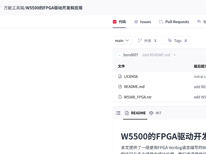
Original project: GitCode, “W5500的FPGA驱动开发和应用: 基于 FPGA 的 W5500 以太网芯片驱动开发项目.” The visible repository describes a Verilog W5500 driver, shows three commits, and identifies an MIT license, but does not expose inspectable HDL source files through the accessible page.
Related project overview: CSDN, “W5500的FPGA驱动开发和应用:为以太网通信打开新大门.” The article describes initialization, transmission, reception, and interrupt-processing modules. It is published under CC 4.0 BY-SA and notes that some content was AI-assisted, so its implementation claims should be confirmed against the downloaded project.
WIZnet product reference: Official W5500 documentation covering the hardwired TCP/IP stack, eight sockets, 32 KB packet memory, 10/100 Ethernet PHY, SPI modes, software resources, and reference hardware.
Register reference: WIZnet ioLibrary_Driver, Ethernet/W5500/w5500.h, containing the official common-register, socket-register, command, interrupt, and buffer-pointer definitions. The project’s Verilog code is not confirmed to use this header; it is used only as an authoritative register reference.
Tags
#W5500 #WIZnet #FPGA #Verilog #Ethernet #IndustrialIoT #Robotics #Education #Maker #Commercial
Verilog FPGA에서 WIZnet W5500으로 Ethernet을 구현하는 방법은?
요약
이 프로젝트는 Verilog로 구현된 FPGA에서 WIZnet W5500 Ethernet controller를 직접 제어하는 구조입니다. MCU 기반 C driver 대신 FPGA가 SPI transaction engine, initialization sequence, register controller, socket state machine, transmit path, receive path, interrupt handling을 구현합니다. W5500은 10/100 Ethernet MAC/PHY, hardwired TCP/IP stack, 8개 hardware socket, internal packet memory를 제공합니다. 이 구조는 명확한 hardware timing과 유선 networking이 필요한 교육 실습, maker prototype, robot controller, industrial data acquisition, commercial product에 적용할 수 있습니다. Visible GitCode repository에서는 Verilog 기반 W5500 driver와 MIT license를 확인할 수 있지만, 실제 HDL file은 노출되지 않아 project-specific code와 performance result는 검증할 수 없습니다.
프로젝트가 하는 일
이 프로젝트는 일반적인 software W5500 driver를 FPGA logic으로 대체합니다. Firmware가 SPI function을 순차적으로 호출하는 대신, Verilog finite-state machine이 W5500의 address, control, data phase를 직접 생성합니다. 관련 project overview는 initialization, transmit, receive, interrupt-processing 기능이 분리되어 있다고 설명하지만, 실제 module boundary와 signal name은 visible repository에서 확인할 수 없습니다.
실제 system data path는 다음과 같습니다.
Sensor, ADC, encoder, camera interface 또는 control logic → FPGA processing pipeline → packet FIFO → W5500 socket controller → SPI master → W5500 → transformer 및 RJ45 → Ethernet network
수신 경로는 반대 방향으로 동작합니다.
Ethernet packet → W5500 Rx buffer → SPI read engine → FPGA receive FIFO → parser, control state machine, processor core 또는 hardware accelerator
이 architecture는 다음 use case에 적용할 수 있습니다.
Industrial IoT: deterministic data acquisition, machine monitoring, protocol gateway, wired telemetry
Robotics: command reception, status reporting, sensor streaming, fixed robotic cell 간 communication
Education: SPI timing, register map, finite-state machine, socket control, Ethernet debugging
Maker: FPGA 기반 UDP instrument, remote I/O, logic-analyzer streaming, network-controlled hardware
Commercial: controlled startup, fault recovery, measurable latency, stable wired interface가 필요한 product
소스 설명은 driver가 Verilog로 작성되었고 여러 프로젝트에 적용되었다고 밝히지만, reproducible benchmark data, FPGA family, resource utilization, clock configuration, test procedure는 제공하지 않습니다. 따라서 performance는 project description에서 추정하지 말고 실제 target board에서 측정해야 합니다.
WIZnet이 들어가는 위치
이 프로젝트에서 사용되는 정확한 WIZnet 제품은 W5500입니다. W5500은 FPGA logic과 physical Ethernet network 사이에 위치합니다.
W5500은 hardwired TCP/IP stack, 10/100 Ethernet MAC and PHY, 8개 independent socket, 32 KB internal Tx/Rx memory를 통합합니다. TCP, UDP, ICMP, IPv4, ARP, IGMP, PPPoE를 지원하며 host interface는 SPI mode 0과 mode 3에서 최대 80 MHz까지 동작합니다.
Architecture의 역할은 다음과 같이 나뉩니다.
FPGA logic
SPI clock, chip select, MOSI, transaction timing 생성
Common register 및 socket register 설정
W5500 Tx/Rx buffer memory 할당
Socket open, connect, listen, send, receive, close 제어
FPGA FIFO와 W5500 memory 사이 payload 이동
Timeout, disconnect, receive, send-complete event 감지
Product-specific packet framing 및 application logic 처리
W5500
10/100 Ethernet physical link 종단
ARP 및 IPv4 processing
Hardware TCP/UDP socket function 실행
Socket state 및 retransmission behavior 유지
FPGA block RAM과 독립적으로 Ethernet payload buffering
Register를 통해 link, socket, interrupt status 제공
W5500은 FPGA application protocol을 대신하지 않습니다. W5500은 transport와 socket offload를 제공합니다. Modbus/TCP framing, proprietary robot command, telemetry encoding, binary measurement format 같은 application protocol은 FPGA logic 또는 embedded processor core에서 구현해야 합니다.
구현 참고 사항
Visible GitCode repository는 project description만 제공하며 Verilog implementation을 inspect할 수 없습니다. 따라서 아래 내용은 unavailable project code를 재현한 것이 아니라 architecture-level integration plan입니다.
FPGA와 W5500 hardware interface
FPGA는 다음 signal을 제공해야 합니다.
SCLK: W5500 SPI clock
MOSI: FPGA에서 W5500으로 전달되는 data
MISO: W5500에서 FPGA로 전달되는 data
SCSn: SPI transaction selection
RSTn: hardware recovery
INTn: socket 및 network event
W5500은 3.3 V에서 동작하며 SPI mode 0과 mode 3을 지원합니다. Ethernet 측에는 권장 transformer 또는 integrated-magnetics RJ45 circuit, termination component, power filtering, PCB layout이 필요합니다. WIZnet은 external transformer 및 integrated RJ45 구현을 위한 reference schematic을 제공합니다.
서로 관련 없는 clock domain 사이를 통과하는 signal에는 synchronizer 또는 asynchronous FIFO를 사용해야 합니다. 특히 INTn은 FPGA system clock과 비동기이며, ADC, camera, motor-control logic 같은 payload producer도 SPI engine과 다른 clock domain에서 동작할 수 있습니다.
SPI transaction engine
W5500 SPI transaction은 address phase, control phase, data phase로 구성됩니다. Control byte는 register 또는 buffer block, read/write direction, transfer mode를 선택합니다.
일반적인 FPGA finite-state machine은 다음 순서로 동작합니다.
Chip select를 assert합니다.
16-bit address를 전송합니다.
Control byte를 전송합니다.
하나 이상의 data byte를 전송하거나 수신합니다.
Chip select를 deassert합니다.
Completion 또는 error flag를 발생시킵니다.
SPI controller는 burst transfer를 지원해야 합니다. Payload byte마다 chip select를 다시 assert하면 bus cycle이 낭비되고 throughput이 제한됩니다. 또한 stalled state machine이 networking pipeline 전체를 잠그지 않도록 timeout mechanism을 포함해야 합니다.
Register initialization
Initialization state machine은 먼저 W5500을 reset하고 VERSIONR을 읽어야 합니다. WIZnet은 W5500 version value를 0x04로 정의합니다.
이후 다음 register를 설정합니다.
GAR: gateway address
SUBR: subnet mask
SHAR: source hardware address
SIPR: source IP address
PHYCFGR: Ethernet PHY configuration 및 link status
Socket별 제어에는 다음 register가 사용됩니다.
Sn_MR: TCP, UDP 또는 MACRAW mode
Sn_CR: OPEN, LISTEN, CONNECT, CLOSE, SEND, RECV command
Sn_SR: current socket state
Sn_IR: connection, receive, disconnect, timeout, send-complete event
Sn_PORT, Sn_DIPR, Sn_DPORT: endpoint configuration
Sn_TX_FSR, Sn_RX_RSR: available Tx space 및 received data size
Sn_TX_WR, Sn_RX_RD: buffer-pointer management
이 register는 FPGA에서 constant 또는 register-address package로 정의해야 합니다. State machine 내부에 numeric literal을 반복해서 작성하면 유지보수와 검증이 어려워집니다.
Transmit 및 receive architecture
Transmit controller는 Sn_TX_FSR을 확인해 충분한 W5500 buffer space가 있는지 확인한 뒤 payload를 기록해야 합니다. 이후 selected socket의 Tx buffer에 payload를 쓰고, Sn_TX_WR을 update한 다음 SEND command를 실행합니다. 마지막으로 SEND_OK 또는 TIMEOUT event를 기다립니다.
Receive controller는 Sn_RX_RSR을 읽고, available byte를 FPGA FIFO로 복사한 다음 Sn_RX_RD를 update하고 RECV command를 실행해야 합니다.
W5500 buffer pointer는 circular structure이므로 pointer wraparound를 정확하게 처리해야 합니다. Continuous stream을 처리하는 application은 downstream FPGA logic이 data를 충분히 빠르게 소비하지 못할 때를 대비해 backpressure 또는 packet-drop policy를 제공해야 합니다.
Performance validation
W5500 Ethernet PHY는 100Base-TX를 지원하고 host SPI interface는 최대 80 MHz를 지원합니다. 그러나 이 수치가 그대로 application throughput이 되는 것은 아닙니다. 실제 transfer에는 SPI address/control overhead, socket-register access, buffer-pointer update, packet header, FPGA scheduling overhead가 포함됩니다.
Performance는 다음 항목을 기준으로 측정해야 합니다.
SPI clock frequency 및 timing margin
Burst length
Payload size
Packets per second
TCP 또는 UDP mode
Active socket 수
FPGA FIFO occupancy
Tx wait time
Rx service latency
Packet loss 및 retransmission count
End-to-end application latency
TCP와 UDP는 별도로 benchmark해야 합니다. UDP는 connection 및 acknowledgement behavior가 없지만 필요할 경우 application이 packet loss와 ordering을 처리해야 합니다. TCP는 connection state와 retransmission을 제공하지만 timing variation이 더 커질 수 있습니다.
실무 팁 / 주의점
낮은 SPI frequency에서 시작해 VERSIONR을 검증하고, timing analysis와 hardware test 이후에만 clock을 높여야 합니다.
RSTn을 FPGA에 연결해 전체 system power cycle 없이 socket 또는 PHY fault를 복구할 수 있게 해야 합니다.
INTn을 synchronizer로 처리하고 socket interrupt와 common interrupt source를 모두 정확하게 clear해야 합니다.
Packet data는 burst read/write를 사용하되 register transaction과 payload-buffer transaction을 구분해야 합니다.
W5500 Tx/Rx memory는 socket마다 동일하게 나누지 말고 실제 traffic requirement에 맞춰 할당해야 합니다.
SPI timeout, socket timeout, disconnect, FIFO overflow, dropped packet, retransmission, link recovery counter를 추가해야 합니다.
Cable removal, switch restart, duplicate IP, malformed command, full FIFO, pointer wraparound, repeated W5500 reset을 테스트해야 합니다.
FAQ
Q: FPGA에 왜 WIZnet W5500을 사용하나요?
A: W5500을 사용하면 FPGA에서 Ethernet MAC, PHY interface, ARP, IPv4, TCP, UDP stack 전체를 RTL로 구현할 필요가 없습니다. FPGA는 명확한 SPI register 및 buffer interface를 제어하고, W5500은 8개 socket과 32 KB packet memory를 제공합니다. Custom hardware data path는 필요하지만 FPGA-native network stack 전체는 필요하지 않은 제품에 적합합니다.
Q: W5500은 FPGA board에 어떻게 연결되나요?
A: Digital interface는 SCLK, MOSI, MISO, SCSn SPI signal과 RSTn, 선택적인 INTn으로 구성됩니다. Physical Ethernet side는 W5500 embedded PHY와 권장 magnetics 및 RJ45 circuit을 사용합니다. SPI mode 0과 mode 3을 지원합니다.
Q: 이 프로젝트에서 W5500은 어떤 역할을 하나요?
A: W5500은 wired Ethernet link, IPv4 transport, hardware TCP/UDP socket, retransmission behavior, packet buffering을 처리합니다. FPGA는 SPI control, register sequencing, socket scheduling, payload movement, application framing, real-time hardware processing을 담당합니다.
Q: 초보자도 이 FPGA 프로젝트를 따라갈 수 있나요?
A: Basic Verilog, synchronous state machine, SPI, FIFO, simulation을 이해하는 학습자에게 적합합니다. 권장 학습 순서는 SPI loopback, W5500 version read, network-register configuration, PHY-link detection, single UDP socket, UDP echo, TCP client 또는 server, interrupt handling, multi-socket scheduling입니다.
Q: FPGA 제어가 MCU W5500 driver보다 항상 빠른가요?
A: 반드시 그렇지는 않습니다. FPGA logic은 predictable scheduling, parallel FIFO, hardware processing pipeline과의 직접 통합을 제공할 수 있습니다. 그러나 application throughput은 W5500 SPI interface, socket operation, packet size, Ethernet protocol behavior에 의해 제한됩니다. 원본 소스에는 검증된 benchmark가 없으므로 MCU와 비교할 때는 동일한 SPI clock, payload, socket mode, network peer, measurement method를 사용해야 합니다.
출처
Original project: GitCode, “W5500的FPGA驱动开发和应用: 基于 FPGA 的 W5500 以太网芯片驱动开发项目.” Visible repository는 Verilog W5500 driver, 3개 commit, MIT license를 설명하지만, accessible page에서는 inspect 가능한 HDL source file을 제공하지 않습니다.
https://gitcode.com/Universal-Tool/59a13
Related project overview: CSDN, “W5500的FPGA驱动开发和应用:为以太网通信打开新大门.” 해당 article은 initialization, transmission, reception, interrupt-processing module을 설명합니다. CC 4.0 BY-SA로 게시되었으며 일부 내용이 AI-assisted라고 명시하므로 implementation claim은 downloaded project와 대조해야 합니다.
https://blog.csdn.net/gitblog_06741/article/details/147210055
WIZnet product reference: Official W5500 documentation covering the hardwired TCP/IP stack, eight sockets, 32 KB packet memory, 10/100 Ethernet PHY, SPI modes, software resources, and reference hardware.
https://docs.wiznet.io/Product/Chip/Ethernet/W5500
Register reference: WIZnet ioLibrary_Driver, Ethernet/W5500/w5500.h, containing official common-register, socket-register, command, interrupt, and buffer-pointer definitions. Project Verilog code가 이 header를 사용한다고 확인된 것은 아니며, authoritative register reference로만 사용했습니다.
https://github.com/Wiznet/ioLibrary_Driver
태그
#W5500 #WIZnet #FPGA #Verilog #Ethernet #SPI #RTL #IndustrialIoT #Robotics #Education #Maker #Commercial