
FPGA high speed TCP/IP communication using W5300 TOE Shield.
This is a verilog FSM project for controlling Wiznet W5300 IC using SiPeed TangNano 9k FPGA and TOE Shield board.
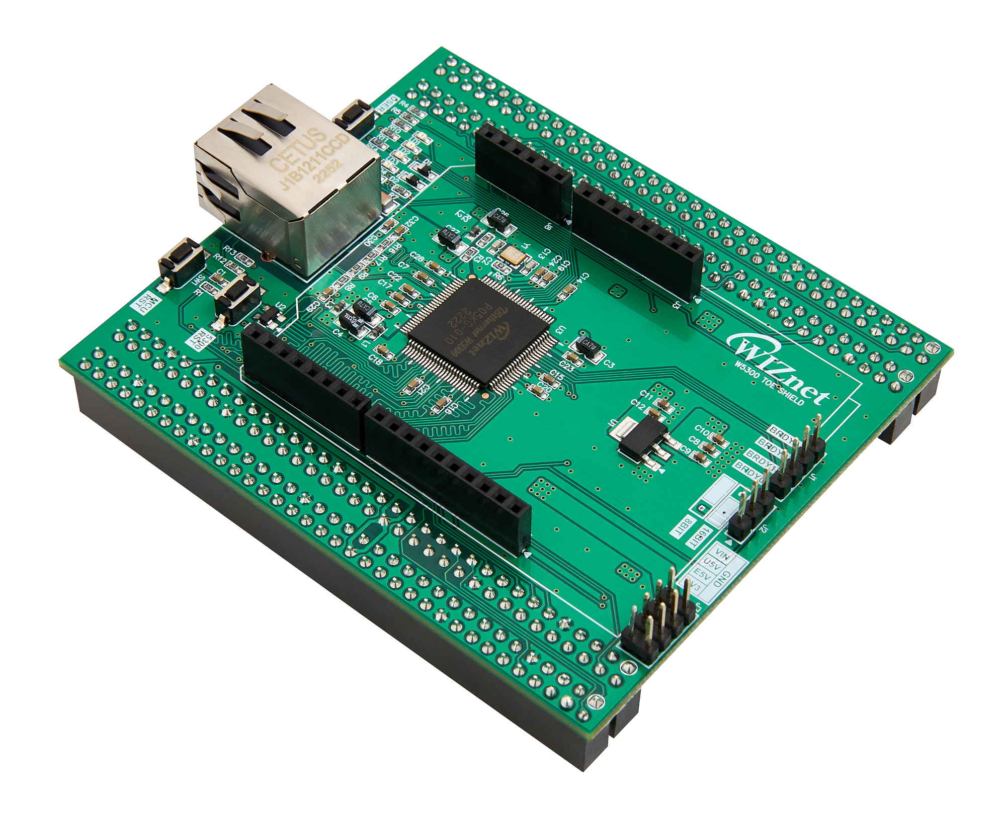
WIZnet - W5300-TOE-Shield
x 1
Python - Python
x 1
HIGH SPEED FPGA ETHERNET SOLUTION BASED ON WIZNET TOE SHIELD.
About.
This project implements a Finite State Machine in Verilog to communicate an FPGA with the hardware network module W5300 in the TOE Shield board.
Project Motivation.
This project is motivated as a learning exercise in verilog to communicate an FPGA with W5300 Network IC. Motivation also comes by the easily availability of low cost components and development boards for both technologies such as the case of W5300 TOE board, which is very handy low cost board although targeted for Nucleo footprint boards in can serve to other boards as well.
Project Description.
Most low cost FPGA chips available do not have Ethernet connectivity such as is the case for Tang Nano 9k board made by SiPeed. This board is very powerful but limiting it to a USB -to Serial connection might stop you from using it in any project that requires Ethernet TCP/IP connectivity. This project aim is to fill the gap or at least show how is possible to build a FSM to communicate easily and get the job done.
Hardware components and setup.
It is well known that FPGA has plenty of I/O pins but small boards like Tang Nano 9k might start to get short if we decide to use a 16 lines data bus. So decision was to use direct addressing mode with 8 bit data bus interface to save some I/O for the other interfaces a project might require.
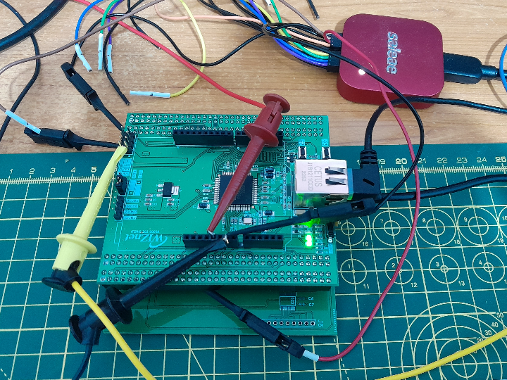
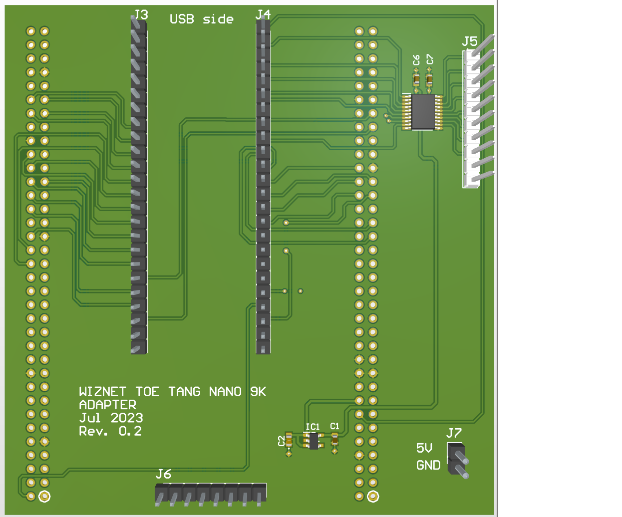
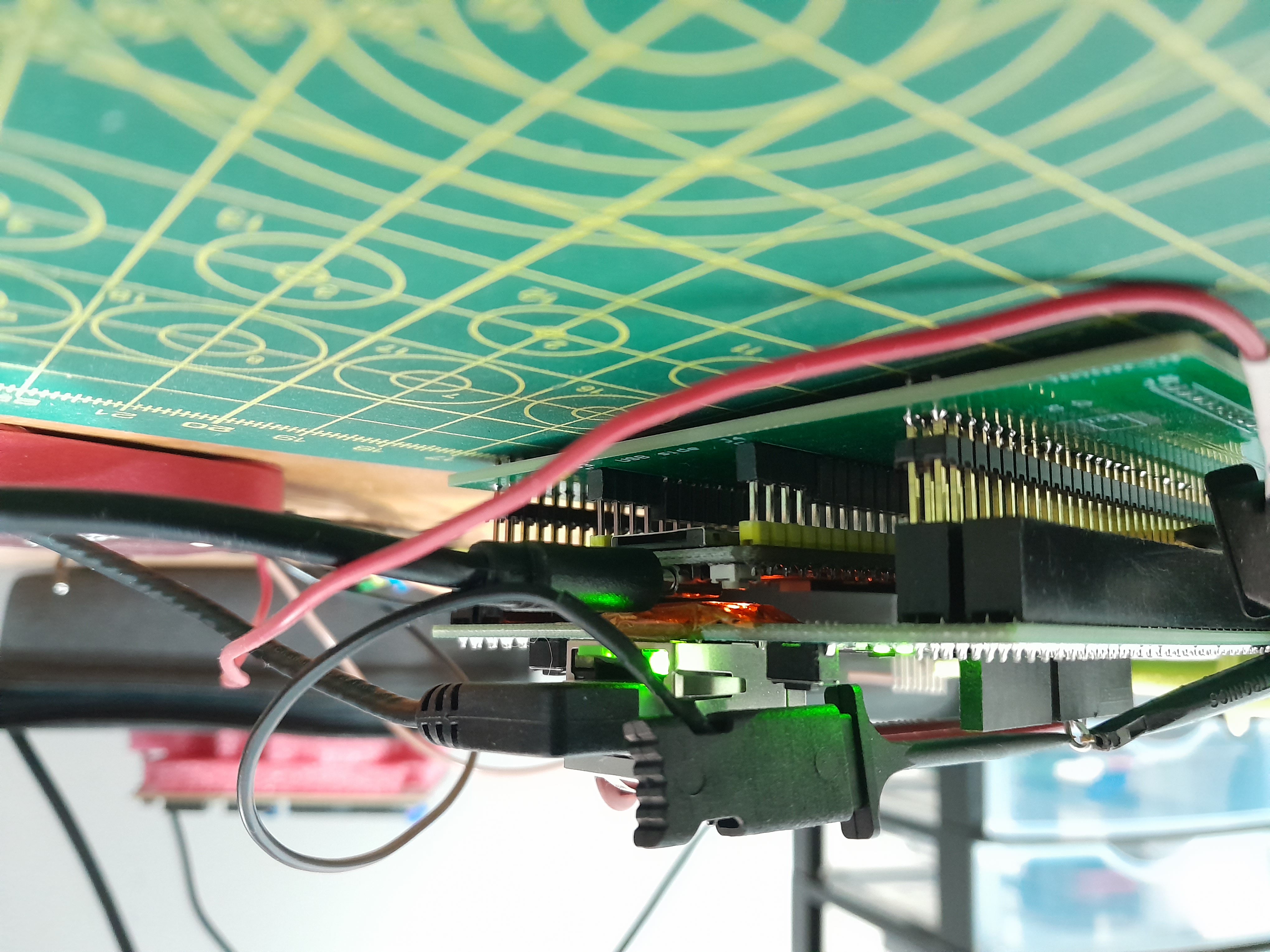
In order to provide a stable test bench for the project, a small base PCB was made to hold the Tang Nano 9k board and the W5300 TOE Shield board.
The schematics are available in github page but the most relevant is the Tang Nano 9k I/O assignment which is given as below.
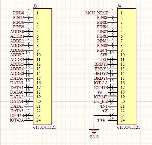
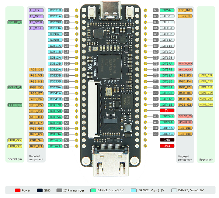
5V and 3.3V are not connected across the two boards as Tang Nano 9K cannot provide the almost 200mA @5V needed for W5300 TOE Shield board.
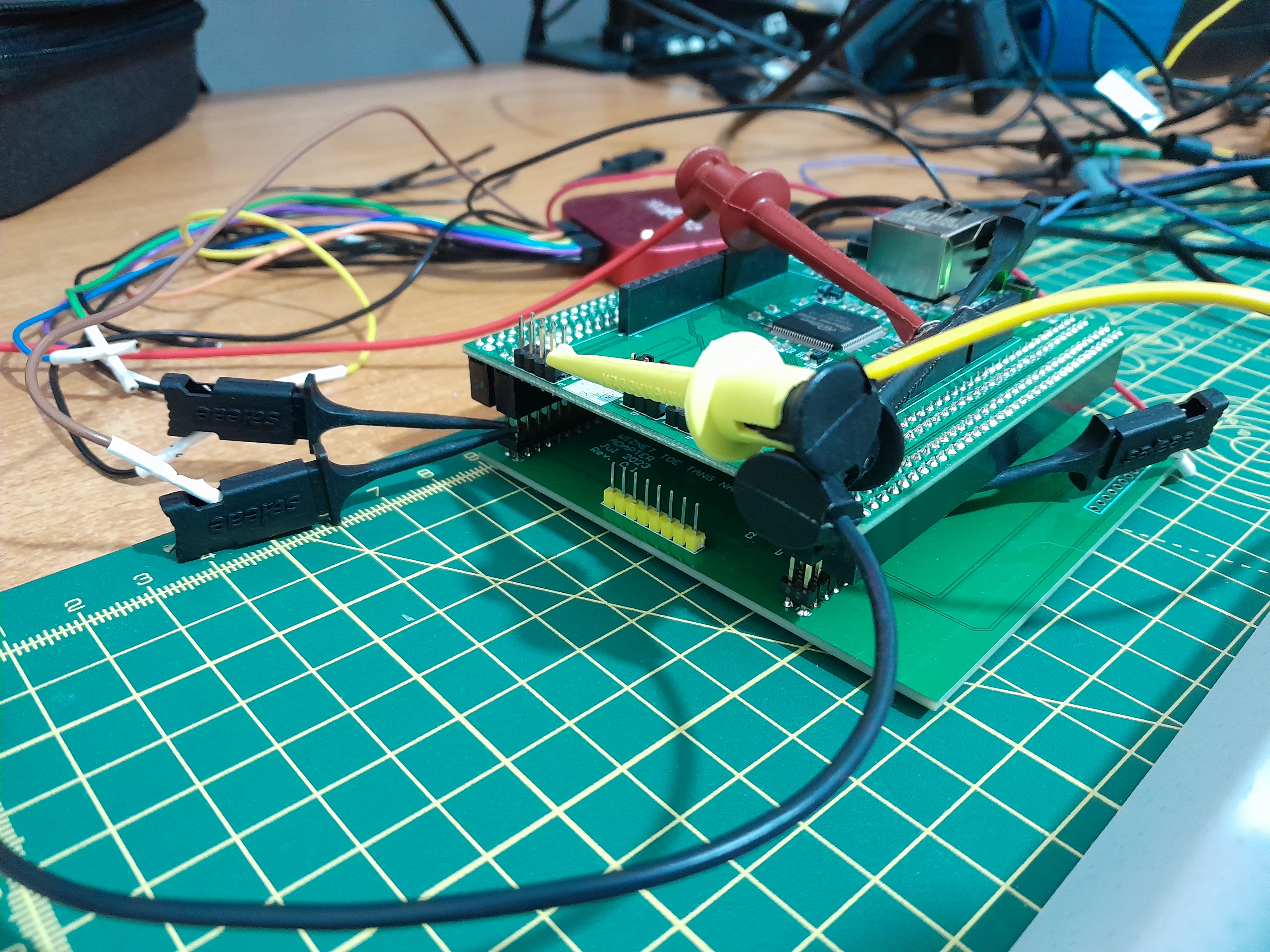
The W5300 TOE board is very handy as it exposes all the I/O, but it is targeted for the Nucleo type of boards and so there is a lot of positions in those two row headers of 72 pins that are not used at all. One problem was how to fit the boards together, it basically reduced to what I was having at hand, I use two long headers made by SAMTEC to give extra high to the board and allow the Tang Nano 9k to fit in between both boards as shown in the following picture.
The long headers are handy to connect logic analyzer probes or the like. For example on the below image I have connected the probes into pins /INT, /RST and USER_BTN (from left to right)
Having a logic analyzer is useful to detect some issues in hardware. But for most of the part you can live with simulations. In this case I was inspecting the /INT pin after a socket interrupt was serviced by the FPGA FSM. Other things like the reset pin is nice to inspect and make sure how it works. For example, the reset works with a helper tiny chip that holds the device in reset for 400 ms as shown below.
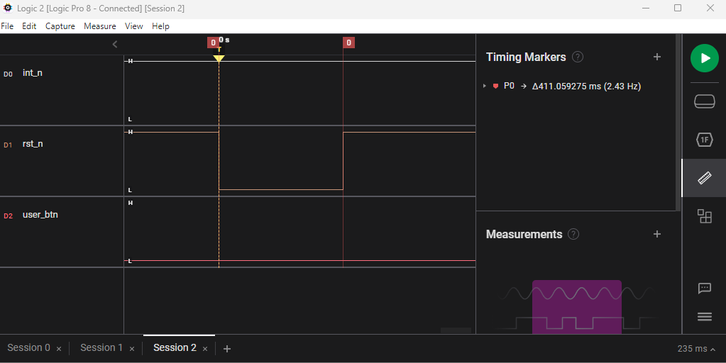
Unfortunately I don't have a 32 channel logic analyzer at hand so we will explore the design by looking at the simulations and of course the demo!
The assignment of I/O is not a task to take it for grant, you can easily blow something if not paying attention. I decide to use signals on banks that have 3.3V support for interfacing the W5300 IC. There are a few signals on Tang Nano 9k board that are 1.8V, so this signals I have routed to an external 1.8v to 3.3v bidirectional level converter to use easily in any external module that requires 3.3V levels.
FPGA project.
For this project I was initially trying to setup open source tools for generating the binary but I end up getting nasty issues not observed in simulation. I was using Lushay lab open source project that integrates to VS code really easy. I then switch to the offical GoWin IDE and got rid of issues. The project can be cloned from the github repo and open directly with the GoWIn FPGA Designer, project is tested with the version shown below.
FSM Design.
Before going streight to describe the design, let's take a look at a demo of what it can do up to the end date of this contest. Look at the video or you tube link..
Basically we can devide the demo in two steps, initialization, which prepare for UDP reception and the process of receiving a packet. The first one is triggered in step 5 of video demo and receiving proces is triggered in step 7.
The FSM has so far 14 states defined in uart_top.v as
localparam                       IDLE =  0;
localparam                       SEND =  1;
localparam                       PROCESS_RX = 2;
localparam                       PROCESS_ADDR_READ = 3;
localparam                       PROCESS_ADDR_PRINT = 4;
localparam                       INIT_ROUTINE = 5;
localparam                       W5300_WRITE_REG = 6;
localparam                       PROCESS_REG_PRINT = 7;
localparam                       PROCESS_REG_READ = 8;
localparam                       W5300_ISR_STATE = 9;
localparam                       W5300_SOCK_RECV_ISR = 10;
localparam                       W5300_READ_SOCK_RECV_SIZE = 11;
localparam                       W5300_RECV_STATE = 12;
localparam                       W5300_RECV_PROCESS = 13;
localparam                       W5300_RECV_COMPLETE = 14;
There are some states that are reused and been transition into them similar to a task, for instance there are two important states to communicate the FPGA with the W5300 IC, basically you will always be either reading a register or writing to a register when it comes to receive or send data from a socket. These two states are W5300_WRITE_REG and PROCESS_REG_READ.
Let's take a close look at what is behind those states to handle the read and write operation.
Single Byte operations.
Basically read or write a register requires two operations on the 8 bit data and address buses, the FPGA has to use the lowest address first. One read or write operation is performed by the module sram_ctrl.v, with a 27MHz clock , the period is about 36ns. For the read operation the minimum time to hold the /CS and /RD lines is 65ns as per w5300 datasheet. Similar for the write operation the times are a bit shorter to around 50ns. So it is evident that we need two clock cycles to do an operation. This timing is controlled in sram_ctrl.v source file. If you find you are working on a different FPGA board with different clock, here is where you want to come and adjust the timing of each operation.
For the write operation, this module make sure there are no bus collisions situations by controlling the /CS and /WR signals and the time data is present on the data bus during the operation. Take a look at the following
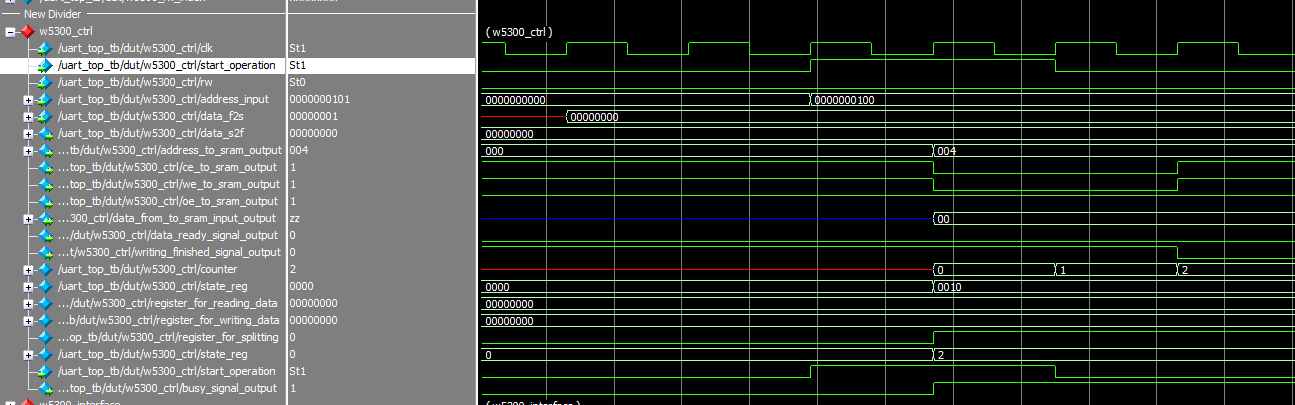
The image shows a Write operation, when the counter becomes 2 it means the data was written and writing_finished_signal_output signal is active low to signal it. The read operation is similar started when the start_operation signal is high level but in the case of read, the data_ready_signal_output signals when the data has been fetch.
As it can be measured from the ModelSim simulation is the timing. For the above read operation, the /CS and /RD lines are held low for about 72ns.
Register Operations.
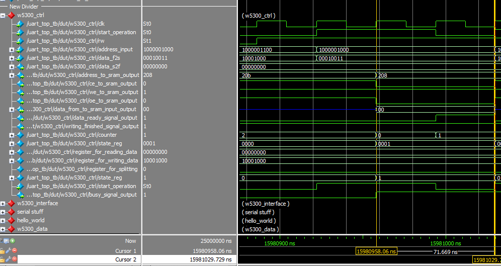
In order to buiild a scalable project, a module controls the read and write operation of WORDS to compose register values. For example setting a Port for UDP ocket requries two 8 bit data write operations as shown below (port value is 5000)
The Write operation completes in around 360ns, the read operation in about 320ns or so.
In our verilog sources, we need to specify the address and data for write operation and setup a couple of control flags for the FSM in order to return to our state after the write/read operation completes. You can send a Write operation for several Words that are on contiguos addresses as the w5300_ctrl module will increment the address by two each time you do a write.
For example to configure the MAC address, we can start the write operation for all bytes by doing
            INIT_W5300_2:                               //
            begin
                address <= SHAR_REG;
                data_16bits <= {8'h00, 8'h08};          // first register is set here
                w5300_regs[0] <= {8'hdc, 8'h01};
                w5300_regs[1] <= {8'h02, 8'h03};
                reg_cnt <= 5'd2;                        // we need to send two more registers
                reg_cnt_sent <= 5'd0;                   // Start sending Index 0 of w5300_regs
                state <= W5300_WRITE_REG;
                init_w5300_state <= INIT_W5300_3;
            end
There is a register for the count, that should be 0 when sending only one register value. Here INIT_W5300_2 State value is 2 and INIT_W5300_3 is 3. Here you can see the transitions simulation and the sub state of init routine changing from 1 to 2 value.
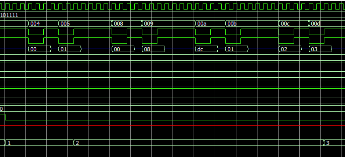
As you can expect the transition from 1 to 2 state is before the signal start to change in the buses.
UART comms - send and receive data over serial line.
The serial port is used initially for a command line utility to test, so there are few states in the FSM that control reading and processing commands as well as printing debug data over the serial lines.
It is kind of similar approach we saw for Register read and write operation, reading is done at all time when the state is in IDLE. Both operation uses a small memory in the FPGA to hold the values to be read/written given by message and message_tx register declarations.
To print the received UDP message we saw in the demo, the following is been done in W5300_RECV_PROCESS state. W5300_RECV_PROCESS:
begin
case(send_serial_flag)
1'b0:
begin
// do something here with packets like sending it out of serial port
if(tx_wr_index > w5300_rx_index - UDP_PACKET_INFO_LEN) begin // let's hardwired this for now to test
send_serial_flag <= 1'b1;
msg_size <= w5300_rx_index - UDP_PACKET_INFO_LEN;
tx_cnt <= 8'd0;
state <= SEND; // go to the SEND state
idle_to_next_state <= 1'b1; // signal that we need to come back to this state
nextstate <= W5300_RECV_PROCESS;
end
else begin
message_tx[tx_wr_index] <= message_w5300_rx[tx_wr_index + UDP_PACKET_INFO_LEN];
tx_wr_index <= tx_wr_index + 1'b1;
end
end
1'b1:
begin
w5300_rx_index <= 8'd0;
tx_wr_index <= 8'd0;
idle_to_next_state <= 1'b0; // signal in this state that we need to first fetch before read
if(socket_recv_value != 17'd0) begin
state <= W5300_RECV_STATE;
end
else begin
state <= W5300_RECV_COMPLETE;
end
end
endcase
endThis state waits until the size has been read, calling W5300_RECV_STATE state as much as needed. When all data is in message_tx memory, the FSM move into SEND state until it send all the bytes before returning to this state.
Processing UDP packet in the demo explained.
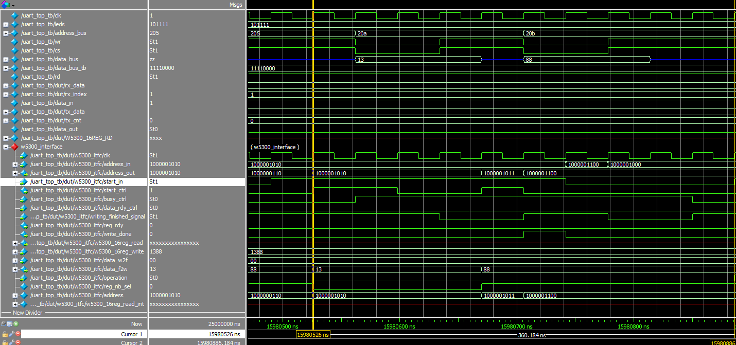
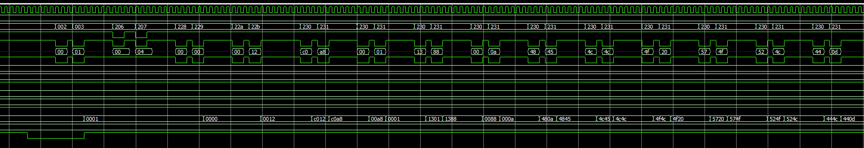
The UDP packet reception starts with the detection of /INT signal. Socket is configured to generate RECV interrupt during the initilization sequence. After detecting the /INT pin is active low, the ISR is been serviced which basically read the size of received data. This will contain UDP packet info and payload. It then clear the RECV interrupt flasg of socket which will internally the w5300 initiate the transition of /INT pin to high if no more interrupts are present.
This can be observed in the following ModelSim simulation.
If you are not familiar you might be wondering how to create this simulations, it is by means of another source in the verilog sources of this project, a file called the test bench. I will explain a few tricks I have done for this project.
Test Bench design and how it works.
The testbench is used to simulate with ModelSim, is a verilog code as well and when creating the project in ModelSim you have to specify it.
The few things about it that I will mention might help you understand its logic and how to modified it if needed.
First you need to generate clock, which is done in this line of code of uart_top_b.v
forever #(c_CLOCK_PERIOD_NS/2) clk = ~clk;There is a task called to takecare of sending bytes on the serial port.
task UART_WRITE_BYTE;So you can use the following to send a carriedge return character for instance.
@(posedge clk);
 UART_WRITE_BYTE(8'h0D);
In order to simulate responses from W5300, the following code take care of the data been place in the bus
  always @(negedge rd)
  begin
    data_bus_tb <= data_bus_16[{data_bus_idx[7:1], nibble}];
    if(nibble == 1'b1) begin
      //last nibble here
      data_bus_idx <= data_bus_idx + 8'd2;    // move to next word
    end
    nibble <= ~nibble;
  end
To prepare for a read operation, specifically, to create the response of reading socket register status after setting it to UDP type, the following code is in the testbench.
      @(posedge clk);
      data_bus_idx <= 8'd0;
      nibble <= 1'b0;
      data_bus_16[0] <= 8'h00;
      data_bus_16[1] <= 8'h22;
And the way I have found to test the interrupt and UDP reception is with the following code.
      // set the w5300 register contents here for our test bench
      @(posedge clk);
      nibble <= 1'b0;
      data_bus_idx <= 8'd0;
      // SET size of packet for UDP. UDP length <8> + DATA length
      data_bus_16[0] <= 8'h00;   // IR_REG0
      data_bus_16[1] <= 8'h01;   // IR_REG1   Bit 0 is S0_INT
      data_bus_16[2] <= 8'h00;   // S0_RX_RSR0
      data_bus_16[3] <= 8'h00;   // S0_RX_RSR1
      data_bus_16[4] <= 8'h00;   // S0_RX_RSR2
      data_bus_16[5] <= 8'h12;   // S0_RX_RSR3   // SIZE = UDP <8> + DATA <10>
      data_bus_16[6] <= 8'hC0;   // UDP Byte Index 0  UDP DESTINATION IP
      data_bus_16[7] <= 8'hA8;   // UDP Byte Index 1
      data_bus_16[8] <= 8'h00;   // UDP Byte Index 2
      data_bus_16[9] <= 8'h01;   // UDP Byte Index 3
      data_bus_16[10] <= 8'h13;   // UDP Byte Index 4   UDP DESTINATION PORT
      data_bus_16[11] <= 8'h88;   // UDP Byte Index 5
      data_bus_16[12] <= 8'h00;   // UDP Byte Index 6
      data_bus_16[13] <= 8'h0A;   // UDP Byte Index 7
      data_bus_16[14] <= 8'h48;   // DATA Byte Index 0  H
      data_bus_16[15] <= 8'h45;   // DATA Byte Index 1  E
      data_bus_16[16] <= 8'h4C;   // DATA Byte Index 2  L
      data_bus_16[17] <= 8'h4C;   // DATA Byte Index 3  L
      data_bus_16[18] <= 8'h4F;   // DATA Byte Index 4  O
      data_bus_16[19] <= 8'h20;   // DATA Byte Index 5
      data_bus_16[20] <= 8'h57;   // DATA Byte Index 6  W
      data_bus_16[21] <= 8'h4F;   // DATA Byte Index 7  O
      data_bus_16[22] <= 8'h52;   // DATA Byte Index 8  R
      data_bus_16[23] <= 8'h4C;   // DATA Byte Index 9  L
      data_bus_16[24] <= 8'h44;   // DATA Byte Index 10  D
      data_bus_16[25] <= 8'h0D;   // DATA Byte Index 11  CR
      @(posedge clk);
      int_n_tb <= 1'b0;
      @(posedge clk);
      @(posedge clk);
      @(posedge clk);
      @(posedge clk);
      @(posedge clk);
      @(posedge clk);
      @(posedge clk);
      @(posedge clk);
      @(posedge clk);
      @(posedge clk);
      int_n_tb <= 1'b1;
Test Station.
A very simple script in python was used to test the UDP socket as shown in the demo video. It is included in sources in github and here for reference.
import socketUDP_IP = "192.168.0.7"
UDP_PORT = 5000
MESSAGE = "Hello World\x0d"print("UDP target IP:", UDP_IP)
print("UDP target port:", UDP_PORT)
print("message:", MESSAGE)data = bytes(MESSAGE, "utf-8")
sock = socket.socket(socket.AF_INET, socket.SOCK_DGRAM) # UDP
sock.sendto(data, (UDP_IP, UDP_PORT))Future Work / Improvements.
The UDP send "routine" has to be developed in order to close the loop and be able to create a loopback example. TCP server/client needs to be developed as well but for most high speed type of projects UDP will be favored as retransmissions sometimes are simple not possible. The loopback example is an interesting one as it allo to measure the speed of the implementation.
Another interesting need that arised during testing and develoing of this project was to be able to control the w5300 reset line from the FPGA. The problem is that the W5300 IC on the TOE shield is controlled by MIC811 IC. One option I am exploring to do while continuing using the TOE shield is to desolder W5300 reset push button and then use an output from FPGA to control the MIC811 input. An inprovement for a next revision of TOE shield might be to use a jumper to disconnect the reset push botton circuit (so then there is no need to de solder component) and providing the input port of MIC811 on the /RST line in the NUCLEO 72 position header. Another possibility might be to include an OR gate that combine the inputs of push button and external reset line
The version 0.1 of the PCB was made without testing the power supply needs of w5300 and it was discovered that the Tang Nano 9k start to present problems to provide the current required to work properly. I have modified the board for removing the 5V line connection and adding external header for 5V input. The /RST line is also disconnected althought the USER_BTN line works and is connected to Tang Nano 9k.
One area of improvement is the location of the Tang Nano underneath the TOE shield. Unfortunately the TOE board came with pins soldered so there was no other option.
Results.
As can be observed in the demo provided, the FPGA can read data from UDP received packet, communication interface between FPGA and W5300 IC is robust and the verilog code is easy to expand. The scope of this project was to provide aloopback example as well to measure network speed of TOE shield. Unfortunately there was not enough time, but nonetheless the project can easily be extended.
Tang Nano 9k and other similar board can use the verilog code to port it to other FPGA platforms as well.
This project open the possibility to combine high speed networking on a low cost FPGA for high speed transfer applications.
Conclusion.
W5300 TOE board but more over the w5300 IC is a great productto provide High Speed Ethernet connectivity to an FPGA, in which the device is performing a task that requires high speed response and connectivity. Allowing the FPGA designer to focus more on the application itself and open new possibilities of using low end devices.
-
Software and Hardware Repository
This repository contains evrything used in this project including verilog source, schematics, gerbers, pictures, etc.

-
base board
Interface board for connecting W5300 TOE shield and Tang Nano 9k boards.
