
Photovoltaic power communication management system design based on Intel SoC FPGA
Photovoltaic power communication management system design based on Intel SoC FPGA

WIZnet - W5500
x 1
0 Preface
The photovoltaic power station uses a large number of photovoltaic panels to complete the conversion from light energy to DC power, and then converts the DC power into 50 Hz AC power using an inverter and transmits it to the grid. There is a huge demand for power control and conversion equipment in the entire photovoltaic power station. The communication management machine, as the equipment connecting each equipment and the power station central console in the power station, controls the downstream Rtu equipment through the control platform, realizes the collection of information such as remote signaling, telemetry, remote control, etc., and feeds back the information to the dispatch center, and then controls the center administrator. Through the processing and analysis of the message, the command to be executed is selected to achieve the goal of the telecontrol output scheduling command.
There are mainly three kinds of communication management machine implementation schemes widely used at present: PowerPC processor + serial port expansion chip architecture, ARM processor architecture, ARM processor + FPGA architecture. Among them: (1) PowerPC processor + serial port expansion chip architecture uses PowerPC processor with communication coprocessor as the core of the system, and uses serial port communication expansion chip to expand up to 16 serial ports for PowerPC. All data processing and operation are completed by PowerPC processor. When all serial ports are used, the whole system runs slowly, and the real-time performance of data is difficult to guarantee. (2) The communication management machine implemented by using a single ARM processor as the core has a simple structure, but the number of serial ports that can be supported is limited by the number of serial ports integrated by the ARM processor itself, generally no more than 6, which cannot meet the requirements of the massive equipment in the photovoltaic power station. need. (3) ARM processor + FPGA architecture uses FPGA to complete serial port expansion, and completes data processing and network protocol implementation based on ARM processor, which is essentially the same as the scheme based on PowerPC + serial port expansion chip. This scheme increases the complexity of the system, but the single performance improvement is not obvious. The problem with the above three solutions is that the system has only one core unit. Once the system is down, the system has to be restarted. If the system is not restored, the entire system is completely disconnected from the power station center console. , unable to receive control commands from the central console.
Based on Intel's new SoC FPGA chip, this paper uses a single SoC FPGA chip to implement the system originally implemented by discrete FPGA and ARM processor, and builds a redundant monitoring system on the FPGA. While improving the system performance, the online recoverability of the system is guaranteed.
1 System modeling
Intel Cyclone V SoC FPGA chip 5CSEMA4U23C6 chip is a SoC chip that integrates high-performance dual-core ARM Cortex-A9 CPU and FPGA on a single chip. It is the core unit of this system.
In this system, the FPGA part of the SoC FPGA chip is mainly responsible for the expansion of the UART interface and the acceleration of the MODBUS protocol.
In the power system , almost all devices support the standard RS485 interface and use the MODBUS protocol to communicate with other devices. In the photovoltaic power station, due to the large number of devices and the large amount of data, one RS485 port of the communication management machine can only communicate with one device at the same time, which leads to a bottleneck in the data transmission speed. In order to solve this problem, multiple MODBUS network ports are often used to realize the management of many devices [2].
After the data of many power equipment is collected by the communication management machine, it needs to exchange data with the central control background of the power station through the Ethernet interface. The system (Hard Process System, HPS) runs a mature Linux operating system to complete.
2 Hardware circuit scheme design
2.1 SoC FPGA configuration circuit design
In order to make the system support remote online upgrade, this system sets the FPGA part of the SoC FPGA to receive the configuration data of the HPS part. The HPS part can receive FPGA configuration files transmitted by serial port or network port. At runtime, the HPS part of the SoC FPGA starts and runs the Linux operating system first, and then configures the FPGA part after the Linux operating system is started. If you need to update the configuration data of the FPGA remotely, you only need to transfer the new FPGA configuration content to the disk managed by the operating system through the network port to replace the original configuration file, and the new configuration file can be used when the system starts up next time. FPGA.
2.2 SoC FPGA startup circuit design
The HPS part of the SoC FPGA runs the Linux operating system, and the HPS supports booting from SD card, Q SPI Flash, and NAND Flash memory. NAND Flash and QSPI Flash memory are generally installed on the circuit board by welding, while the SD card is detachable and can be read and written on the PC separately. In the industrial field, if the equipment system is damaged and the system needs to be re-programmed, the QSPI Flash and NAND Flash can only be programmed online with a PC because they are soldered on the PCB, while the SD card can be programmed with a pre-programmed SD card. Cards are replaced, thus saving on-site maintenance effort.
2.3 RS485 interface circuit design
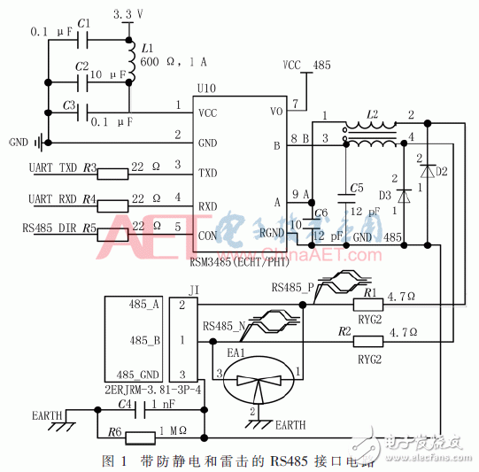
As an industrial device, the communication interface of the communication management machine may withstand various shocks, including strong common-mode voltage, high-voltage static electricity, and lightning strikes. Therefore, the protection measures for the communication interface are very important. In this system, the RSM3485 module is used to complete the bidirectional conversion from TTL level to RS485 level. The RSM3485 module implements a standard RS485 interface, with ESD protection, short-circuit or open-circuit failure protection, built-in 120 kΩ pull-up and pull- down resistors , twisted pair output, and provides ESD discharge functions of ±4 kV under contact and ±8 kV under air discharge. At the same time, a lightning protection circuit is designed to prevent damage to the communication interface in the case of lightning strikes. The interface circuit diagram is shown in Figure 1.
2.4 Design of Ethernet interface scheme
The power system communication management machine requires the provision of active and standby dual network ports to ensure that when one of the network ports fails, the other network port can continue to transmit necessary data. The 5CSEMA4U23C6 chip provides two Gigabit Ethernet MACs by default, but these two MACs are managed by the HPS part. In order to ensure the reliability of the network port, even when the ARM part of the system is down, the spare network port can In normal work, only one MAC layer is used in the design, which is driven by HPS, and the other network port is implemented by the integrated Ethernet communication chip W5500 controlled by NIOS II soft core.
The W5500 chip is a single-chip TCP/IP protocol chip implemented by hardware, supports 8 Socket ports, and is very convenient and reliable to use. Using NIOS II to control the W5500 to complete the Ethernet transmission, even if the HPS works abnormally, the NIOS II CPU in the FPGA can continue to send and receive data through the W5500 to ensure the stable operation of the standby network port.
3 SoC FPGA application architecture design
Since SoC FPGA is an innovative architecture that integrates FPGA and high-performance HPS, it can make full use of the powerful data processing capability of HPS, flexible customization features on the FPGA side, and high-speed communication bridge between HPS and FPGA during design. Various tasks are reasonably allocated to the FPGA or HPS according to their characteristics, and the two cooperate to achieve the highest performance.
The FPGA side mainly realizes the expansion of the UART communication interface and the backup system based on the NIOS II processor. The HPS side mainly realizes the conversion between a large number of data processing and communication protocols. Figure 2 is a block diagram of the functional division on the SoC FPGA.

3.1 FPGA logic design
The logic part of the FPGA side implements 16 UART communication control units that support automatic identification of MODBUS frames, as shown in Figure 3. Each unit is composed of CRC check logic, serial port data transceiver buffer, core control state machine and MODBUS frame identification logic. Under the control of the core control state machine, each unit automatically completes the sending and receiving of MODBUS data frames and the generation of data check codes, and transmits the data received and sent by MODBUS with the HPS via the Avalon MM Slave interface.
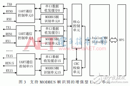
Figure 4 is the working state transition diagram of the enhanced UART communication control unit that supports automatic identification of MODBUS frames when it receives data. The whole state machine consists of idle state (IDLE), receiving data state (GET_DATA), receiving timeout state (TIMEOUT), receiving byte data completion state (GET_BYTE), and frame transmission completion state (FRAME_DONE).
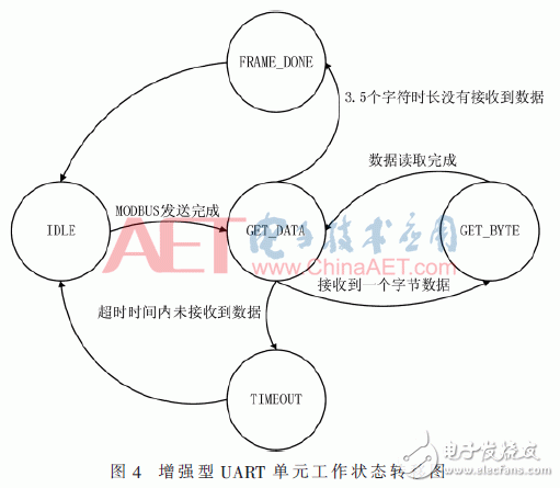
When the host sends a MODBUS request frame, the module enters the data receiving state (GET_DATA), and jumps into the receiving byte completion state (GET_BYTE) every time a byte is received. When the frame end judgment signal is valid, it indicates a frame of data When the reception is completed, it enters the frame reception completion state. Determine whether the current frame is correct by comparing the CRC data field in the received data frame with the check data generated by the CRC check unit in the FPGA for the frame. Then send an interrupt request to HPS through the FPGA and HPS interconnection bridge, and report the verification result of the current frame. The Linux driver on the HPS side will complete the corresponding processing according to the verification result. If the verification is correct, the frame data will be read. And submit it to the upper MODBUS protocol layer for further analysis and processing, if the frame is wrong, discard the frame and enter the error processing program.
3.2 Linux software design
The HPS in the SoC FPGA runs the Linux operating system and runs the application program of the communication management machine on the Linux system. The application program mainly includes three parts, namely MODBUS protocol master station, IEC104 protocol slave station, and protocol conversion program between MODBUS and IEC104 protocol. Among them, the MODBUS protocol master station runs the open source Libmodbus protocol stack to complete the sending and receiving of MODBUS commands and data.
Libmodbus protocol stack is a free and open source MODBUS protocol stack that supports MODBUS protocol master and slave functions. Because this system uses hardware logic circuit on the FPGA side, some functions of the MODBUS protocol have been realized, such as frame end judgment, CRC check and so on. Therefore, the Libmodbus protocol stack has been cut and optimized to a certain extent, and the part of receiving and verifying the underlying data frame is removed, and only its instruction and data parsing part is used. This is also the advantage of this system. The bottom layer of the MODBUS protocol is realized through the FPGA side hardware. content, reducing the workload of the processor, so that the processor can easily complete the support for up to 16 ports based on the MODBUS protocol.
In order to facilitate the control of the 16-port MODBUS accelerators on the FPGA side, a separate process is opened on the Linux side for the control of the 16-port MODBUS accelerators. Then execute the corresponding processing code according to the obtained port state. The program flow is shown in Figure 5.
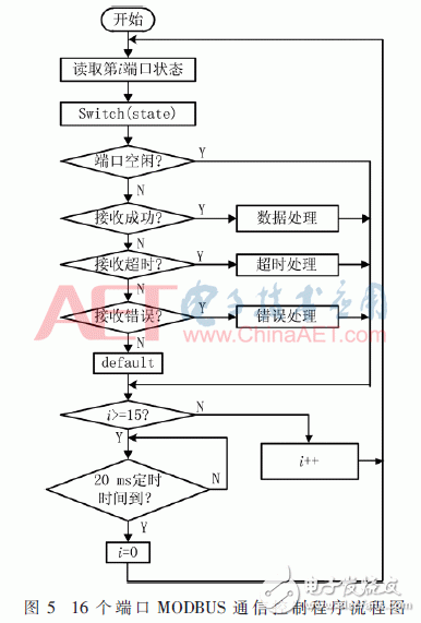
Idle state: When the state of a port is found to be idle, it indicates that the port has completed a round of data transmission and reception correctly. Before a new communication command arrives, the port will be in an idle state, that is, it does not need to send data, nor does it need to send data. To receive data, the MODBUS port is in an idle state.
Received successfully: When it is found that a certain port has successfully received the returned data, the processing of the received data will start, and after completion, it will enter the status query of the next port.
Receive timeout: When the query finds that a port has no response within the set response time, it will return the receive timeout status. If the timeout state is detected, the system starts to process the timeout. After the receiving timeout processing is completed, enter the status query work of the next port.
Receive error: When an error is found in receiving data from a certain port, the receive error processing will be performed. When the receiving error processing is completed, enter the status query work of the next port. The code framework for this part of the task is as follows:
for(i=0;i《=15;i++)
{
port_state=mdp_state_read(port_num); // Read the specified port state
switch(port_state)
{
case NO_STATE: break; // no ready port
case RX_DONE: // Receive data successfully
…// Receive data processing code module
break;
case RX_TIMEOUT: // receive timeout
…// Receive timeout port processing code module
break;
case RX_ERROR: // receive error
…// Receive error port handling code module
break;
default:
printf("default %d\n\n", port_num); // default is misread
Error handling, setting the status register to the error flag
FPGA_WR16((port_num《《8 | 128), 1);
}// After reading the 16th port, return to port 0 to read
if(port_num == 15) port_num = 0;
else port_num ++; // The port number is incremented by 1
}
usleep(30000); // release CPU permissions
3.3 NIOS II Standby System Software Design
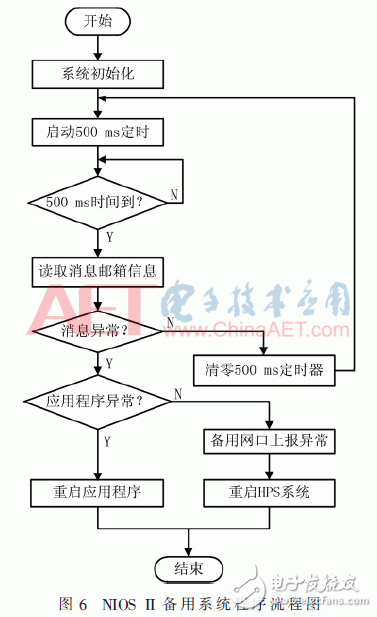
Normally, the NIOS II CPU is in the standby state. If the NIOS II CPU does not receive a status message within the set time, it means that the software system on the HPS system side has crashed. The operating system is down or the application is abnormal. If the application is abnormal, trigger the Linux side security monitoring software to restart the application; if the operating system is abnormal, start the standby network port to report the current system fault information to the power station center console, and restart the HPS through hardware reset. Figure 6 is the program flow chart of the NIOS II backup system.
4 System performance analysis
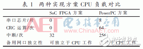
Table 1 takes 16 RS485 ports, each port completes a data read to the device on the bus every 500 ms, and the average length of each communication data frame is 64 B as an example to analyze the system solution within 1 s (referred to as SoC FPGA). Solution) and PowerPC+ serial port expansion chip ST16C2550 solution (referred to as PowerPC solution) are different in the number of serial port chips, CPU CRC operation transactions, CPU processing interrupt times, and the independence of the standby network port.
5 Conclusion
The photovoltaic power communication management machine system based on Intel SoC FPGA designed in this paper gives full play to the advantages of FPGA in processing multi-channel parallel data communication, greatly reduces the interrupt overhead of embedded processors in managing communication transactions in traditional solutions, and reduces the The total number of RS485 ports supporting the MODBUS protocol in a single system is increased, which can effectively simplify the layout and wiring of the communication network of the photovoltaic power station. At the same time, due to the programmable characteristics of FPGA, the system can be upgraded by reprogramming the FPGA without changing the hardware circuit, solving the problems of multiple devices and large data volume in the photovoltaic power system, and increasing the system performance. scope of application.