Multi-protocol long-distance low-power IoT gateway hardware planning
Multi-protocol long-distance low-power IoT gateway hardware planning

Wang Xinyu (1981-), male, intermediate engineer, research direction: wireless communication, radio frequency circuit design and Internet of Things; Qiu Mangang, male, assistant engineer, research direction: Internet of things, intelligent control, application of wireless communication technology.
Abstract : Aiming at the existence of multiple specifications such as Zigbee, BLE, Wireless M-Bus, 6LoWPAN , etc. in IoT network applications, a multi-protocol long-distance low-power IoT gateway hardware planning plan is proposed. The gateway selects NXP's KW41Z and TI's CC1310 two multi-protocol wireless SoC chips as the center to establish hardware channels, and adds SKYWORKS' SKY66112-11 and SKY66115-11 power amplifier front-end modules. The gateway can complete the interconnection between the cloud server and the IoT network. The test results show that the gateway has a good wireless connection function and is very suitable for IoT network applications under multi-standard protocols.
0 Introduction
IoT (Internet of Things, Internet of Things) is a network communication technology that is developing rapidly now. The IoT application architecture includes the perception layer, the network layer and the application layer from the bottom up. The perception layer is composed of many sensor nodes, which collect data and transmit data through wireless transmission technology (WiFi, BLE, Zigbee, etc.). The transmission layer uses the existing 2G/3G/4G, wired broadband and other communication technologies to widen the data transmission interval of the perception layer. The application layer is primarily responsible for analyzing and processing data and providing users with an application interface. The primary effect of the IoT gateway is to complete the protocol conversion between the sensing layer and the network layer, so that the data of the sensing node can be transmitted to the backend server through the Internet. Because most of the existing low-power sensor nodes use standard communication protocols such as Zigbee and BLE, in order to achieve data exchange between sensor nodes with different protocols, a multi-protocol IoT gateway is required .
1 System plan
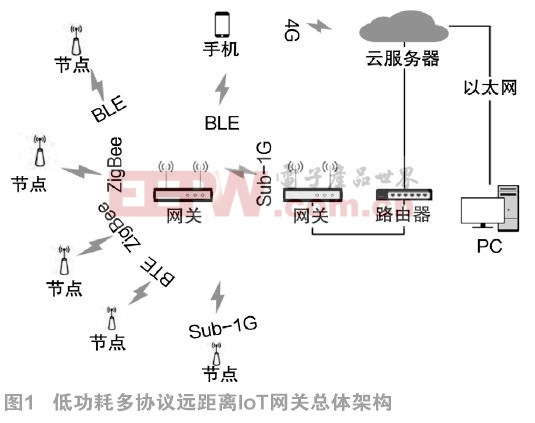
This paper proposes a low-power multi-protocol remote IoT gateway, which adopts SoC RF chip design, which can realize the integration of multiple IoT protocol networks. The gateway can support BLE, Zibgee, 6Lowpan and Sub-1GHz private protocols, etc., and data exchange can be performed directly or directly between sensors of different protocols. The low-power IoT gateway planned in this project can be powered by batteries, thus eliminating the traditional high-energy WiFi connection method. Because the amount of data in the sensor network is very small, we can choose a low-speed network for data transmission. Figure 1 shows the overall architecture of a low-power multi-protocol remote-interval IoT gateway.

The IoT gateway in Figure 1 always plays the role of a central bridge in the entire system. The gateway can support two common 2.4 GHz protocols, BLE and Zigbee, and can also process the Sub-1 GHz communication protocol. The data of each IoT node can be forwarded through the gateway. and interaction. Zigbee nodes or BLE nodes can send data to the gateway, through the gateway, the sensor data is encapsulated into TCP/IP data packets, and sent to the cloud server through Ethernet. Remote users can obtain data from the server through a PC or a mobile terminal, and can send the control data to the gateway through the cloud server, and then the gateway sends it to the corresponding sensor node.
The multi-protocol IoT gateway can not only complete the above-mentioned long-distance data processing, but also carry out localized data exchange. For example, the BLE node node can send data and control commands to the gateway, and then the gateway performs protocol conversion and sends it to the Zigbee node for data exchange. This communication no longer needs to go through the cloud server, and when there is no network connection to the cloud, the IoT network communication in the area can also be carried out. Now all mobile phones support BLE low-power Bluetooth communication, and mobile phones can also be connected to the gateway directly through the BLE communication interface without connecting to the cloud server, and interact with the sensor nodes through the APP software.
In applications where wiring is inconvenient, IoT gateways can be powered by batteries. In the case of long distance, multiple gateways can be cascaded through the Sub-1GHz channel. After multi-level connection, it is finally connected to the cloud server through the wired network. The scale of application has been greatly expanded.
2 Hardware Planning
In order to reduce the cost and volume of the system, this paper uses the SoC RF chip solution. The latest KW41Z [1] chip from NXP is used to complete the 2.4 GHz frequency band protocol processing, and TI's CC1310 [2] chip is used to complete the Sub-1 GHz frequency band protocol processing. Select WIZnet company's hardware network protocol stack W5500 [3] to complete the Ethernet data transmission.
2.1 KW41Z circuit planning
KW41Z is an ultra-low-power, highly-integrated SoC radio chip launched by NXP. The hardware supports both Bluetooth Low Energy (BLE) v4.2 and IEEE® 802.15.4 physical layer. Select 48 MHz ARM Cortex-M0+ core, up to 512 KB Flash and 128 KB SRAM. Receive sensitivity (802.15.4) is -100 dBm and programmable transmitter output power up to +3.5 dBm. Built-in balun single-ended output, the circuit structure is simple.
The 2.4 GHz band signal is greatly affected by the environment, so it is necessary to increase the transmission power and reception sensitivity. This article selects the SKY66112-11[4] power amplifier chip from Skyworks. The chip can provide a maximum output power of 21 dBm, 8dB receiving gain. Internal integrated transceiver switching RF switch, supporting two antenna outputs. The operating frequency range is 2.4 GHz to 2.45 GHz, and the supply voltage is 1.8 to 3.6 V.

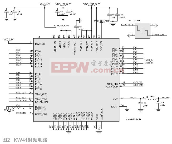
The RF circuit design of KW41Z is shown in Figure 2. We use the DC-DC power supply mode. The DCDC_LP (pin 11) and DCDC_LN (pin 12) of KW41Z are connected to the external 10μH inductor of the DC-DC circuit. VDD_1P45 (pin 15) internal 1.45 V power output, supply operating power to the internal RF circuit, VDD_RF (pin 32, 35, 36) is connected to the 1.45V power supply, add decoupling capacitors to each pin . VDD_1P8 (pin 14) internal 1.8 V power output, supply power to I/O and peripherals. VDDCDC_IN (pin 10) internal DC-DC power input, connected to external 3.3 V power supply. ANT (pin 33) RF input and output pins, an external low-pass filter (C8, C9 and L2) is required to reduce the harmonics and stray radiation power of the output RF signal.
The SKY66112-11 amplifier module circuit is shown in Figure 3, because the input and output ports of the SKY66112-11 chip are both 50Ω, the output of the KW41Z can be directly connected to RF_IN (pin 21). VCC1 (pin 16) and VCC2 (pin 14) are the internal PA and LNA power supply needs to be routed independently, and each pin adds decoupling% &&&&&&% independently. CRX (pin 2), CTX (pin 17), CPS (pin 15), CSD (pin 3) and ANT_SEL (pin 4) are logic control pins, which are connected to the I/O pins of KW41Z. ANT1 (pin 8) is connected to the internal PCB antenna through a low-pass filter, and ANT2 (pin 6) is connected to the SMA seat through a low-pass filter circuit, and then connected to the external rod antenna.

2.2 CC1310 circuit planning
CC1310 is a sub-1GHz SoC RF chip launched by TI. The chip supports multiple physical layer specifications, Wireless M-Bus, IEEE 802.15.4g and custom specifications. It is very suitable for multi-protocol gateway applications. CC1310 integrates a powerful 48MHz ARM Cortex-M3 microcontroller and dedicated wireless controller (ARM Cortex-M0), 128 KB Flash and 20 KB RAM. The maximum output power is 15 dBm, and the excellent receiving function can reach the receiving sensitivity of -124 dBm in the form of long interval. The CC1310 has a very high level of integration and can operate with only a few peripherals.

In order to adapt to different working environments, it is necessary to add a PA amplifier externally to increase the transmission interval. This article selects the SKY66115-11 [5] power amplifier chip from Skyworks . SKY66115-11 integrates power amplifier and RF switch, operating frequency is 400 MHz~510 MHz, operating voltage is 2.5~3.6 V, and the maximum output power is +20 dBm.
